

Configuration and Remote System Upgrades in Cyclone IV ... - Altera
Configuration and Remote System Upgrades in Cyclone IV ... - Altera
Configuration and Remote System Upgrades in Cyclone IV ... - Altera

You also want an ePaper? Increase the reach of your titles
YUMPU automatically turns print PDFs into web optimized ePapers that Google loves.
Chapter 8: <strong>Configuration</strong> <strong>and</strong> <strong>Remote</strong> <strong>System</strong> <strong>Upgrades</strong> <strong>in</strong> <strong>Cyclone</strong> <strong>IV</strong> Devices 8–47<br />
<strong>Configuration</strong><br />
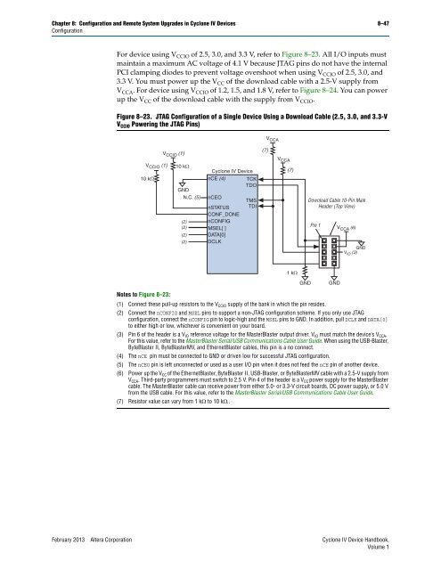
For device us<strong>in</strong>g V CCIO of 2.5, 3.0, <strong>and</strong> 3.3 V, refer to Figure 8–23. All I/O <strong>in</strong>puts must<br />
ma<strong>in</strong>ta<strong>in</strong> a maximum AC voltage of 4.1 V because JTAG p<strong>in</strong>s do not have the <strong>in</strong>ternal<br />
PCI clamp<strong>in</strong>g diodes to prevent voltage overshoot when us<strong>in</strong>g V CCIO of 2.5, 3.0, <strong>and</strong><br />
3.3 V. You must power up the V CC of the download cable with a 2.5-V supply from<br />
V CCA. For device us<strong>in</strong>g V CCIO of 1.2, 1.5, <strong>and</strong> 1.8 V, refer to Figure 8–24. You can power<br />
up the V CC of the download cable with the supply from V CCIO.<br />
Figure 8–23. JTAG <strong>Configuration</strong> of a S<strong>in</strong>gle Device Us<strong>in</strong>g a Download Cable (2.5, 3.0, <strong>and</strong> 3.3-V<br />
V CCIO Power<strong>in</strong>g the JTAG P<strong>in</strong>s)<br />
V CCIO (1)<br />
10 kΩ<br />
Notes to Figure 8–23:<br />
V CCIO (1)<br />
10 kΩ<br />
GND<br />
N.C. (5)<br />
(2)<br />
(2)<br />
(2)<br />
(2)<br />
<strong>Cyclone</strong> <strong>IV</strong> Device<br />
nCE (4) TCK<br />
TDO<br />
nCEO<br />
nSTATUS<br />
CONF_DONE<br />
nCONFIG<br />
MSEL[ ]<br />
DATA[0]<br />
DCLK<br />
(1) Connect these pull-up resistors to the VCCIO supply of the bank <strong>in</strong> which the p<strong>in</strong> resides.<br />
(2) Connect the nCONFIG <strong>and</strong> MSEL p<strong>in</strong>s to support a non-JTAG configuration scheme. If you only use JTAG<br />
configuration, connect the nCONFIG p<strong>in</strong> to logic-high <strong>and</strong> the MSEL p<strong>in</strong>s to GND. In addition, pull DCLK <strong>and</strong> DATA[0]<br />
to either high or low, whichever is convenient on your board.<br />
(3) P<strong>in</strong> 6 of the header is a VIO reference voltage for the MasterBlaster output driver. VIO must match the device’s VCCA. For this value, refer to the MasterBlaster Serial/USB Communications Cable User Guide. When us<strong>in</strong>g the USB-Blaster,<br />
ByteBlaster II, ByteBlasterMV, <strong>and</strong> EthernetBlaster cables, this p<strong>in</strong> is a no connect.<br />
(4) The nCE p<strong>in</strong> must be connected to GND or driven low for successful JTAG configuration.<br />
(5) The nCEO p<strong>in</strong> is left unconnected or used as a user I/O p<strong>in</strong> when it does not feed the nCE p<strong>in</strong> of another device.<br />
(6) Power up the VCC of the EthernetBlaster, ByteBlaster II, USB-Blaster, or ByteBlasterMV cable with a 2.5-V supply from<br />
VCCA. Third-party programmers must switch to 2.5 V. P<strong>in</strong> 4 of the header is a VCC power supply for the MasterBlaster<br />
cable. The MasterBlaster cable can receive power from either 5.0- or 3.3-V circuit boards, DC power supply, or 5.0 V<br />
from the USB cable. For this value, refer to the MasterBlaster Serial/USB Communications Cable User Guide.<br />
(7) Resistor value can vary from 1 k to 10 k..<br />
February 2013 <strong>Altera</strong> Corporation <strong>Cyclone</strong> <strong>IV</strong> Device H<strong>and</strong>book,<br />
Volume 1<br />
TMS<br />
TDI<br />
(7)<br />
V CCA<br />
V CCA<br />
(7)<br />
1 kΩ<br />
GND<br />
Download Cable 10-P<strong>in</strong> Male<br />
Header (Top View)<br />
P<strong>in</strong> 1<br />
GND<br />
V CCA (6)<br />
GND<br />
V IO (3)


