

Configuration and Remote System Upgrades in Cyclone IV ... - Altera
Configuration and Remote System Upgrades in Cyclone IV ... - Altera
Configuration and Remote System Upgrades in Cyclone IV ... - Altera

You also want an ePaper? Increase the reach of your titles
YUMPU automatically turns print PDFs into web optimized ePapers that Google loves.
8–20 Chapter 8: <strong>Configuration</strong> <strong>and</strong> <strong>Remote</strong> <strong>System</strong> <strong>Upgrades</strong> <strong>in</strong> <strong>Cyclone</strong> <strong>IV</strong> Devices<br />
<strong>Configuration</strong><br />
f For more <strong>in</strong>formation about the USB-Blaster download cable, refer to the USB-Blaster<br />
Download Cable User Guide. For more <strong>in</strong>formation about the ByteBlaster II download<br />
cable, refer to the ByteBlaster II Download Cable User Guide.<br />
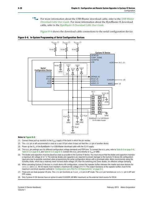
Figure 8–6 shows the download cable connections to the serial configuration device.<br />
Figure 8–6. In-<strong>System</strong> Programm<strong>in</strong>g of Serial <strong>Configuration</strong> Devices<br />
Notes to Figure 8–6:<br />
Serial<br />
<strong>Configuration</strong> Device<br />
DATA<br />
DCLK<br />
nCS<br />
ASDI<br />
V CCIO (1) V CCIO (1) V CCIO (1)<br />
10 kΩ 10 kΩ 10 kΩ<br />
10 kΩ<br />
GND<br />
10 pf<br />
(5)<br />
3.3 V 3.3 V<br />
3.3 V<br />
3.3 V<br />
(5)<br />
GND<br />
GND<br />
10 pf<br />
GND<br />
GND<br />
10 pf<br />
<strong>Cyclone</strong> <strong>IV</strong> Device<br />
nSTATUS<br />
CONF_DONE<br />
nCONFIG<br />
nCE<br />
nCEO<br />
DATA[0] (6)<br />
DCLK (6)<br />
nCSO (7)<br />
ASDO (7)<br />
3.3 V (3)<br />
MSEL[ ] (4)<br />
(1) Connect these pull-up resistors to the VCCIO supply of the bank <strong>in</strong> which the p<strong>in</strong> resides.<br />
(2) The nCEO p<strong>in</strong> is left unconnected or used as a user I/O p<strong>in</strong> when it does not feed the nCE p<strong>in</strong> of another device.<br />
(3) Power up the VCC of the ByteBlaster II or USB-Blaster download cable with the 3.3-V supply.<br />
(4) The MSEL p<strong>in</strong> sett<strong>in</strong>gs vary for different configuration voltage st<strong>and</strong>ards <strong>and</strong> POR time. To connect the MSEL p<strong>in</strong>s, refer to Table 8–3 on page 8–8,<br />
Table 8–4 on page 8–8, <strong>and</strong> Table 8–5 on page 8–9. Connect the MSEL p<strong>in</strong>s directly to VCCA or GND.<br />
(5) The diodes <strong>and</strong> capacitors must be placed as close as possible to the <strong>Cyclone</strong> <strong>IV</strong> device. You must ensure that the diodes <strong>and</strong> capacitors ma<strong>in</strong>ta<strong>in</strong><br />
a maximum AC voltage of 4.1 V. The external diodes <strong>and</strong> capacitors are required to prevent damage to the <strong>Cyclone</strong> <strong>IV</strong> device AS configuration<br />
<strong>in</strong>put p<strong>in</strong>s due to possible overshoot when programm<strong>in</strong>g the serial configuration device with a download cable. <strong>Altera</strong> recommends us<strong>in</strong>g the<br />
Schottky diode, which has a relatively lower forward diode voltage (VF) than the switch<strong>in</strong>g <strong>and</strong> Zener diodes, for effective voltage clamp<strong>in</strong>g.<br />
(6) When cascad<strong>in</strong>g <strong>Cyclone</strong> <strong>IV</strong> devices <strong>in</strong> a multi-device AS configuration, connect the repeater buffers between the master <strong>and</strong> slave devices for<br />
DATA[0] <strong>and</strong> DCLK. All I/O <strong>in</strong>puts must ma<strong>in</strong>ta<strong>in</strong> a maximum AC voltage of 4.1 V. The output resistance of the repeater buffers must fit the<br />
maximum overshoot equation outl<strong>in</strong>ed <strong>in</strong> “<strong>Configuration</strong> <strong>and</strong> JTAG P<strong>in</strong> I/O Requirements” on page 8–5.<br />
(7) These p<strong>in</strong>s are dual-purpose I/O p<strong>in</strong>s. The nCSO p<strong>in</strong> functions as FLASH_nCE p<strong>in</strong> <strong>in</strong> AP mode. The ASDO p<strong>in</strong> functions as DATA[1] p<strong>in</strong> <strong>in</strong> AP <strong>and</strong><br />
FPP modes.<br />
(8) Only <strong>Cyclone</strong> <strong>IV</strong> GX devices have an option to select CLKUSR (40 MHz maximum) as the external clock source for DCLK.<br />
<strong>Cyclone</strong> <strong>IV</strong> Device H<strong>and</strong>book, February 2013 <strong>Altera</strong> Corporation<br />
Volume 1<br />
10 pf<br />
P<strong>in</strong> 1<br />
GND<br />
GND<br />
ByteBlaster II or USB Blaster<br />
10-P<strong>in</strong> Male Header<br />
N.C. (2)<br />
CLKUSR (8)


