

Configuration and Remote System Upgrades in Cyclone IV ... - Altera
Configuration and Remote System Upgrades in Cyclone IV ... - Altera
Configuration and Remote System Upgrades in Cyclone IV ... - Altera

You also want an ePaper? Increase the reach of your titles
YUMPU automatically turns print PDFs into web optimized ePapers that Google loves.
8–56 Chapter 8: <strong>Configuration</strong> <strong>and</strong> <strong>Remote</strong> <strong>System</strong> <strong>Upgrades</strong> <strong>in</strong> <strong>Cyclone</strong> <strong>IV</strong> Devices<br />
<strong>Configuration</strong><br />
If you configure a master device with an SFL design, the master device enters user<br />
mode even though the slave devices <strong>in</strong> the multiple device cha<strong>in</strong> are not be<strong>in</strong>g<br />
configured. The master device enters user mode with a SFL design even though the<br />
CONF_DONE signal is externally held low by the other slave devices <strong>in</strong> cha<strong>in</strong>.<br />
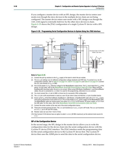
Figure 8–29 shows the JTAG configuration of a s<strong>in</strong>gle <strong>Cyclone</strong> <strong>IV</strong> device with a SFL<br />
design.<br />
Figure 8–29. Programm<strong>in</strong>g Serial <strong>Configuration</strong> Devices In-<strong>System</strong> Us<strong>in</strong>g the JTAG Interface<br />
Serial <strong>Configuration</strong><br />
Device VCCIO (1)<br />
DATA<br />
DCLK<br />
nCS<br />
ASDI<br />
Notes to Figure 8–29:<br />
V CCIO (1)<br />
10 kΩ<br />
V CCIO (1)<br />
10 kΩ<br />
25 Ω (7)<br />
10 kΩ<br />
GND<br />
N.C. (5)<br />
(2)<br />
<strong>Cyclone</strong> <strong>IV</strong> Device<br />
nCE (4)<br />
TCK<br />
TDO<br />
nSTATUS<br />
CONF_DONE<br />
nCONFIG<br />
MSEL[ ]<br />
DATA[0]<br />
DCLK<br />
nCSO (8)<br />
ASDO (8)<br />
(1) Connect the pull-up resistors to the VCCIO supply of the bank <strong>in</strong> which the p<strong>in</strong> resides.<br />
(2) The MSEL p<strong>in</strong> sett<strong>in</strong>gs vary for different configuration voltage st<strong>and</strong>ards <strong>and</strong> POR time. To connect MSEL for AS<br />
configuration schemes, refer to Table 8–3 on page 8–8, Table 8–4 on page 8–8, <strong>and</strong> Table 8–5 on page 8–9. Connect<br />
the MSEL p<strong>in</strong>s directly to VCCA or GND.<br />
(3) P<strong>in</strong> 6 of the header is a VIO reference voltage for the MasterBlaster output driver. The VIO must match the VCCA of the<br />
device. For this value, refer to the MasterBlaster Serial/USB Communications Cable User Guide. When us<strong>in</strong>g the<br />
ByteBlasterMV download cable, this p<strong>in</strong> is a no connect. When us<strong>in</strong>g USB-Blaster, ByteBlaster II, <strong>and</strong> EthernetBlaster<br />
cables, this p<strong>in</strong> is connected to nCE when it is used for AS programm<strong>in</strong>g, otherwise it is a no connect.<br />
(4) You must connect the nCE p<strong>in</strong> to GND or driven low for successful JTAG configuration.<br />
(5) The nCEO p<strong>in</strong> is left unconnected or used as a user I/O p<strong>in</strong> when it does not feed the nCE p<strong>in</strong> of another device.<br />
(6) Power up the VCC of the EthernetBlaster, ByteBlaster II, USB-Blaster, or ByteBlasterMV cable with a 2.5- V VCCA supply.<br />
Third-party programmers must switch to 2.5 V. P<strong>in</strong> 4 of the header is a VCC power supply for the MasterBlaster cable.<br />
The MasterBlaster cable can receive power from either 5.0- or 3.3-V circuit boards, DC power supply, or 5.0 V from<br />
the USB cable. For this value, refer to the MasterBlaster Serial/USB Communications Cable User Guide.<br />
(7) Connect the series resistor at the near end of the serial configuration device.<br />
(8) These p<strong>in</strong>s are dual-purpose I/O p<strong>in</strong>s. The nCSO p<strong>in</strong> functions as FLASH_nCE p<strong>in</strong> <strong>in</strong> AP mode. The ASDO p<strong>in</strong> functions<br />
as DATA[1] p<strong>in</strong> <strong>in</strong> AP <strong>and</strong> FPP modes.<br />
(9) Resistor value can vary from 1 k to 10 k.<br />
(10) Only <strong>Cyclone</strong> <strong>IV</strong> GX devices have an option to select CLKUSR (40 MHz maximum) as the external clock source for<br />
DCLK.<br />
ISP of the <strong>Configuration</strong> Device<br />
In the second stage, the SFL design <strong>in</strong> the master device allows you to write the<br />
configuration data for the device cha<strong>in</strong> <strong>in</strong>to the serial configuration device with the<br />
<strong>Cyclone</strong> <strong>IV</strong> device JTAG <strong>in</strong>terface. The JTAG <strong>in</strong>terface sends the programm<strong>in</strong>g data<br />
for the serial configuration device to the <strong>Cyclone</strong> <strong>IV</strong> device first. The <strong>Cyclone</strong> <strong>IV</strong><br />
device then uses the ASMI p<strong>in</strong>s to send the data to the serial configuration device.<br />
<strong>Cyclone</strong> <strong>IV</strong> Device H<strong>and</strong>book, February 2013 <strong>Altera</strong> Corporation<br />
Volume 1<br />
nCEO<br />
TMS<br />
TDI<br />
Serial<br />
Flash<br />
Loader<br />
CLKUSR<br />
(9)<br />
V CCA<br />
(10)<br />
V CCA<br />
(9)<br />
1 kΩ<br />
GND<br />
Download Cable 10-P<strong>in</strong> Male<br />
Header (Top View)<br />
P<strong>in</strong> 1<br />
GND<br />
V CCA (6)<br />
GND<br />
V IO (3)


