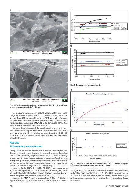
a) a) transmissivity [%] b) 60 50 40 30 20 10 0 200 400 600 800 1000 1200 wavelength (nm) 1% GNPC 0,25% CNT 1%GNPC +0,1%CNT 1%GNPC+ 0,05%CNT b) transmissivity [%] 90 80 70 60 50 40 30 20 10 0 200 400 600 800 1000 1200 wavelenght (nm) 0,1 % GNPB 0,3 % GNPB 0,5 % GNPB Fig. 2. Transparency measurements a) Fig. 1. ITME image: a) graphene nanoplatelets GNP-B, 2-5 um, b) graphene nanoplatelets GNP-C 2-25 um To measure transparency optical spectrometer was used. Length <strong>of</strong> emitted waves varied from 1200 to 200 nm, but waves shorter than 300 nm were blocked by PET substrate. Prepared samples were compared with samples containing 0,25 wt% multiwalled carbon nanotubes (MWCNTs) and mixtures connecting 1wt% GNPs-C with 0,05 or 0,1wt%MWCNTs. To verify <strong>the</strong> resistance <strong>of</strong> <strong>the</strong> conductive layer to cyclic bending mechanical fatigue tests were conducted. Prepared samples were compared with similar samples based on 0,25 wt% MWCNTs in 8 wt% PMMA 10 um layer and with 160 nm ITO on borosilicate glass. Results Transparency measurements Using GNPs in screen printed layers allows wavelengths with <strong>the</strong> same intensity pass through (in contrast to layers based on CNTs). This interesting property is characteristic for <strong>the</strong> GNPs layers and can by used in various types <strong>of</strong> sensors. Relatively high transparency <strong>of</strong> <strong>the</strong> layer containing <strong>the</strong> filler <strong>of</strong> carbon nanotubes for <strong>the</strong> waves in <strong>the</strong> upper measuring range is reduced by 50 percent for <strong>the</strong> wave length <strong>of</strong> 300 nm (Fig. 2a). Layer <strong>of</strong> 1wt% GNPs-C + 0,05wt% CNT has resistance at 80 kΩ/□. Transparency <strong>of</strong> 32% is sufficient for this layer to serve as an electrode for electroluminescent displays and shall be fur<strong>the</strong>r investigated as a possible fotovoltaic cell. Layers with GNP B loading varying from 0,1% to 0,5% have higher transmissivity. Resistance <strong>of</strong> 0,1 GNP B layer is 2,2 M Ω/□ 98 b) Resistance [kΩ/ □ ] 14 12 10 8 6 4 2 0 Results <strong>of</strong> mechanical fatigue tests. 0 10000 20000 30000 40000 50000 60000 70000 80000 number <strong>of</strong> cycles 2%GNPC 0,25% CNT Fig. 3. Results <strong>of</strong> mechanical fatigue tests: a) ITO based samples, b) comparison MWCNT layers with GNPC layer for layer based on Dupont 8155 matrix. Layers with PMMA-based matrix have resistance <strong>of</strong> 1,5 M Ω/□. High transparency <strong>of</strong> 75…80% will allow to print layers on elastic photovoltaic applications such as transparent conductive layers supporting classic electrodes. Elektronika 6/2012
a) b) Fig. 4. ITME image: a) graphene nanoplatelets agglomeration, b) screen printing GNP-C layers on PET film Mechanical properties <strong>of</strong> elastic graphene films Investigation proved that graphene layers have <strong>the</strong> same mechanical resistance as carbon nanotubes layers. After nearly 75 000 cycles, <strong>the</strong> paths resistance <strong>of</strong> paste based on GNPs changed +/- 2% and <strong>the</strong> resistance <strong>of</strong> <strong>the</strong> paste paths based on carbon nanotubes, after initial improvement after <strong>the</strong> first 2000 cycles, consistently declined slightly, although value was higher than starting one. High mechanical resistance makes <strong>the</strong>m suitable to use in elastic fotovoltaic applications. Resistance <strong>of</strong> ITO based samples investigated in <strong>the</strong> same way changes after very first cycles. Fur<strong>the</strong>r bending quickly leads to destruction <strong>of</strong> <strong>the</strong> layer. Summary GNPs based layers prepared with screen printing technology proved to have good mechanical resistance and high transparency. GNPs agglomerates were observed in investigated samples and <strong>the</strong>y are <strong>the</strong> cause <strong>of</strong> <strong>the</strong> layer’s resistance raise. Fur<strong>the</strong>r investigation needs to be done to observe how such situation can be avoided. First experiments on carbon nanotubes layers showed that using dispersants prevents agglomerating. Without agglomerates appearing in <strong>the</strong> samples, conductivity improves consistently. References [1] R. Hilderman, “SIGNS OF CLIMATE CHANGE,” Mo<strong>the</strong>r Earth News, p. 60, 2011. [2] C. Perrow, “Fukushima and <strong>the</strong> inevitability <strong>of</strong> accidents,” Bulletin <strong>of</strong> <strong>the</strong> Atomic Scientists, vol. 67, pp. 44–52, 2011. [3] J. E. Z. Innocent, N. Jari, and N. Matti, “Effects <strong>of</strong> a hydropower plant on Coleopteran diversity and abundance in <strong>the</strong> Udzungwa Mountains, Tanzania,” Biodiversity & Conservation, vol. 13, pp. 1453–1464, 2004. [4] M. de Lucas, M. Ferrer, M. J. Bechard, and A. R. Muñoz, “Griffon vulture mortality at wind farms in sou<strong>the</strong>rn Spain: Distribution <strong>of</strong> fatalities and active mitigation measures,” Biological Conservation, vol. 147, pp. 184–189, 2012. [5] U. L. D. Bach, “Solid-state dye-sensitized mesoporous TiO... solar cells with high photon-to-electron conversion,” Nature, vol. 395, p. 583, 1998. [6] K. Schulze, B. Maennig, K. Leo, Y. Tomita, C. May, J. Hupkes, E. Brier, E. Reinold, and P. Bauerle, “Organic solar cells on indium tin oxide and aluminum doped zinc oxide anodes,” Applied Physics Letters, vol. 91, p. 073521, 2007. [7] K. Fehse, K. Walzer, K. Leo, W. Lövenich, and A. Elschner, “Highly Conductive Polymer Anodes as Replacements for Inorganic Materials in High-Efficiency Organic Light-Emitting Diodes,” Advanced Materials, vol. 19, pp. 441–444, 2007. [8] K. S. Novoselov, A. K. Geim, S. V. Morozov, D. Jiang, M. I. Katsnelson, I. V. Grigorieva, S. V. Dubonos, and A. A. Firsov, “Two-dimensional gas <strong>of</strong> massless Dirac fermions in graphene,” Nature, vol. 438, pp. 197–200, 2005. [9] Y. Zhang, Y.-W. Tan, H. L. Stormer, and P. Kim, “Experimental observation <strong>of</strong> <strong>the</strong> quantum Hall effect and Berry’s phase in graphene,” Nature, vol. 438, pp. 201–204, 2005. [10] K. S. Kim, Y. Zhao, H. Jang, S. Y. Lee, J. M. Kim, K. S. Kim, J.-H. Ahn, P. Kim, J.-Y. Choi, and B. H. Hong, “Large-scale pattern growth <strong>of</strong> graphene films for stretchable transparent electrodes,” Nature, vol. 457, pp. 706–710, 2009. [11] L. Changgu, W. Xiaoding, J. W. Kysar, and J. Honel, “Measurement <strong>of</strong> <strong>the</strong> Elastic Properties and Intrinsic Strength <strong>of</strong> Monolayer Graphene,” Science, vol. 321, pp. 385–388, 2008. [12] W. Supinda, A. D. Dmitriy, S. Sasha, P. Richard, J. Inhwa, H. B. D. Ge<strong>of</strong>frey, E. Guennadi, W. Shang-En, C. Shu-Fang, L. Chuan-Pu, T. N. SonBinh, and S. R. Rodney, “Graphene−Silica Composite Thin Films as Transparent Conductors,” Nano Letters, vol. 7, pp. 1888– 1892, 2007. [13] R. R. Nair, P. Blake, A. N. Grigorenko, K. S. Novoselov, T. J. Booth, T. Stauber, N. M. R. Peres, and A. K. Geim, “Fine structure constant defines visual transparency <strong>of</strong> graphene,” Science (New York, N.Y.), vol. 320, pp. 1308–1308, 2008. [14] X. Wang, L. Zhi, and K. Mullen, “Transparent, Conductive Graphene Electrodes for Dye-Sensitized Solar Cells,” Nano Letters, vol. 8, pp. 323–327, 2008/01/01 2007. [15] L. Xiaolin, Z. Guangyu, B. Xuedong, S. Xiaoming, W. Xinran, W. Enge, and D. Hongjie, “Highly conducting graphene sheets and Langmuir– Blodgett films,” Nature Nanotechnology, vol. 3, pp. 538–542, 2008. [16] L. Gomez De Arco, Y. Zhang, C. W. Schlenker, K. Ryu, M. E. Thompson, and C. Zhou, “Continuous, highly flexible, and transparent graphene films by chemical vapor deposition for organic photovoltaics,” ACS Nano, vol. 4, pp. 2865–2873, 2010. [17] Y.-Y. Choi, S. J. Kang, H.-K. Kim, W. M. Choi, and S.-I. Na, “Multilayer graphene films as transparent electrodes for organic photovoltaic devices,” Solar Energy Materials & Solar Cells, vol. 96, pp. 281–285, 2012. [18] K.-Y. Shin, J.-Y. Hong, and J. Jang, “Flexible and transparent graphene films as acoustic actuator electrodes using inkjet printingElectronic supplementary information (ESI) available: A detailed experimental procedure, characterization, preparation <strong>of</strong> graphene films, AFM, TEM image <strong>of</strong>,” Chemical Communications, vol. 47, pp. 8527– 8529, 2011. [19] F. Torrisi, T. Hasan, W. Wu, Z. Sun, A. Lombardo, T. S. Kulmala, G.-W. Hsieh, S. Jung, F. Bonaccorso, P. J. Paul, D. Chu, and A. C. Ferrari, “Inkjet-printed graphene electronics,” ACS Nano, vol. 6, pp. 2992–3006, 2012. [20] J. M. Sibiński Maciej, Znajdek Katarzyna, Słoma Marcin, Guzowski Bartłomiej, “Carbon nanotube transparent conductive layers for solar cells application,” Optica Applicata, vol. XLI, pp. 375–381, 2011. [21] J. Ping, Y. Wang, K. Fan, J. Wu, and Y. Ying, “Direct electrochemical reduction <strong>of</strong> graphene oxide on ionic liquid doped screen-printed electrode and its electrochemical biosensing application,” Biosensors & Bioelectronics, vol. 28, pp. 204–209, 2011. [22] L. Zhang, Y. Li, L. Zhang, D.-W. Li, D. Karpuzov, and Y.-T. Long, “Electrocatalytic Oxidation <strong>of</strong> NADH on Graphene Oxide and Reduced Graphene Oxide Modified Screen-Printed Electrode,” International Journal <strong>of</strong> Electrochemical Science, vol. 6, pp. 819–829, Mar 2011. [23] M. Qian, T. Feng, H. Ding, L. Lin, H. Li, Y. Chen, and Z. Sun, “Electron field emission from screen-printed graphene films,” Nanotechnology, vol. 20, Oct 21 2009. [24] D. W. Zhang, X. D. Li, S. Chen, H. B. Li, Z. Sun, X. J. Yin, and S. M. Huang, Graphene Nanosheet Counter-Electrodes for Dye-Sensitized Solar Cells, 2010. Elektronika 6/2012 99