

Proceedings of the European Summer School of Photovoltaics 4 â 7 ...
Proceedings of the European Summer School of Photovoltaics 4 â 7 ...
Proceedings of the European Summer School of Photovoltaics 4 â 7 ...

Create successful ePaper yourself
Turn your PDF publications into a flip-book with our unique Google optimized e-Paper software.
Photoelectrical properties <strong>of</strong> photovoltaic structures<br />
based on CdTe/ZnO<br />
EUNIKA Zielony 1) , PAULINA Kamyczek 1) , PIOTR Biegański 1) , EWA Płaczek-Popko 1) ,<br />
RAFAŁ Pietruszka 2) , GRZEGORZ Łuka 2) , MAREK Godlewski 2)<br />
1)<br />
Wrocław University <strong>of</strong> Technology, Institute <strong>of</strong> Physics<br />
2)<br />
Institute <strong>of</strong> Physics, Institute <strong>of</strong> Physics Polish Academy <strong>of</strong> Sciences, Warsaw<br />
<strong>Photovoltaics</strong> continues to be one <strong>of</strong> <strong>the</strong> fastest growing industries,<br />
with annual increase beyond 40% [1]. Photovoltaic (PV)<br />
solar cells convert incoming solar radiation directly into electricity<br />
and produce electricity as each conventional source <strong>of</strong> energy,<br />
but <strong>the</strong>y are very attractive for <strong>the</strong>y are environment friendly.<br />
Zinc oxide (ZnO) is nowadays worldwide extensively studied<br />
for optoelectronics and photovoltaics application. It is predicted<br />
that <strong>the</strong>re will be a mass production <strong>of</strong> conducting ZnO layers as<br />
transparent electrodes in solar cells. It is said that ZnO layers will<br />
soon replace indium transparent oxide (ITO) because <strong>of</strong> high cost<br />
and limited supply <strong>of</strong> indium. Yet <strong>the</strong>re is ano<strong>the</strong>r very attractive<br />
field <strong>of</strong> ZnO application. It may be used as <strong>the</strong> n-type partner<br />
for <strong>the</strong> organic materials. There is a bright future in front <strong>of</strong> <strong>the</strong><br />
PV cells based on such a hybrid structures for <strong>the</strong>ir flexibility and<br />
a very low cost <strong>of</strong> production.<br />
The use <strong>of</strong> ZnO in <strong>the</strong> novel electronic and PV devices demands<br />
low or extremely low processing temperature [2–4]. There<br />
are many different technologies used to obtain ZnO layers. These<br />
are chemical vapor deposition (CVD), molecular beam epitaxy<br />
(MBE), sputtering, electron-beam evaporation, pulse laser deposition<br />
(PLD), hydro<strong>the</strong>rmal method and many o<strong>the</strong>rs, however<br />
<strong>the</strong>se techniques are unsuitable for <strong>the</strong> aforementioned applications<br />
as <strong>the</strong>y are run at too high temperature. In this context<br />
<strong>the</strong> Low Temperature Atomic Layer Deposition method (LT ALD)<br />
technique has proven to be <strong>the</strong> most promising [5]. Moreover,<br />
<strong>the</strong> technique is fairly cheap and allows ZnO growth with atomic<br />
resolution.<br />
Experiment<br />
The subject <strong>of</strong> investigations was a test semiconductor cell based<br />
on ZnO grown by ALD method on CdTe substrate. The structure<br />
<strong>of</strong> <strong>the</strong> studied sample is depicted in Fig. 1. The undoped layer <strong>of</strong><br />
ZnO is <strong>the</strong> n-type partner for p-type CdTe whereas <strong>the</strong> ZnO:Al<br />
layer is transparent conductive layer. The thickness <strong>of</strong> <strong>the</strong> ZnO<br />
layers was determined from interference spectra <strong>of</strong> reflectance<br />
measurements [6].<br />
oxygen precursor. Zinc oxide is created as a result <strong>of</strong> a doubleexchange<br />
chemical reaction that takes place at <strong>the</strong> surface:<br />
Zn(C 2<br />
H 5<br />
) 2<br />
+ H 2<br />
O → ZnO + 2C 2<br />
H 6<br />
Substrate temperature was varied between 60°C and 240°C. For<br />
dimethylzinc (DMZn) as zinc precursor a growth temperature could<br />
be reduced to a room temperature [7].<br />
Rectifying properties <strong>of</strong> <strong>the</strong> ZnO/CdTe junction have been<br />
investigated by current-voltage (I-V) characteristics measured<br />
in darkness and after illumination. Spectral characteristics<br />
<strong>of</strong> photocurrent have been carried out within spectral range <strong>of</strong><br />
300…1100 nm using PV Quantum Efficiency system, Bentham<br />
U.K. From <strong>the</strong> I-V measurements series resistance (R s<br />
) was<br />
calculated. From <strong>the</strong> spectral characteristics <strong>of</strong> photocurrent<br />
spectral sensitivity was determined. Additionally, based on <strong>the</strong><br />
spectral characteristics <strong>of</strong> photocurrent <strong>the</strong> thickness <strong>of</strong> <strong>the</strong> layers<br />
was determined.<br />
Results<br />
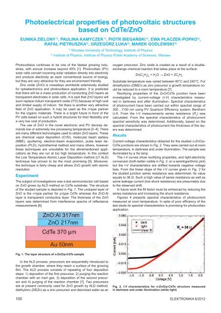
Current-voltage characteristics obtained for <strong>the</strong> studied n-ZnO/p-<br />
CdTe junctions are shown in Fig. 2. They were carried out at room<br />
temperature, in darkness and under illumination. The sample was<br />
illuminated by a Xe lamp.<br />
The I-V curves show rectifying properties, and light-electricity<br />
conversion (both better visible in Fig. 3. on a semilogarithmic plot)<br />
but <strong>the</strong> I-V characteristics are shifted towards negative voltage<br />
bias. From <strong>the</strong> linear slope <strong>of</strong> <strong>the</strong> I-V curves given in Fig. 2 for<br />
<strong>the</strong> studied junction series resistance was determined. Its value<br />
equals to 36 Ω. Such a high value <strong>of</strong> series resistance as well as<br />
some leakage current (low shunt resistance) are presumably due<br />
to <strong>the</strong> observed shift.<br />
In future work <strong>the</strong> fill factor must be enhanced by reducing <strong>the</strong><br />
series resistance and increasing <strong>the</strong> shunt resistance.<br />
Figures 4 presents spectral characteristics <strong>of</strong> photocurrent<br />
measured at room temperature. In spite <strong>of</strong> poor efficiency <strong>of</strong> <strong>the</strong><br />
test diode its spectral characteristics is promising for photovoltaic<br />
application.<br />
Fig. 1. The layer structure <strong>of</strong> n-ZnO/p-CdTe sample<br />
In <strong>the</strong> ALD process, precursors are sequentially introduced to<br />
<strong>the</strong> growth chamber, where <strong>the</strong>y reach a surface <strong>of</strong> <strong>the</strong> growing<br />
film. The ALD process consists <strong>of</strong> repeating <strong>of</strong> four deposition<br />
steps: 1) deposition <strong>of</strong> <strong>the</strong> first precursor, 2) purging <strong>the</strong> reaction<br />
chamber with an inert gas, 3) deposition <strong>of</strong> <strong>the</strong> second precursor<br />
and 4) purging <strong>of</strong> <strong>the</strong> reaction chamber [7]. Two precursors<br />
are at present commonly used for ZnO growth by ALD method:<br />
diethylzinc (DEZn) as a zinc precursor and deionized water as an<br />
Fig. 2. I-V characteristics for n-ZnO/p-CdTe structure measured<br />
in darkness and under illumination (white light)<br />
100<br />
Elektronika 6/2012


