

Proceedings of the European Summer School of Photovoltaics 4 â 7 ...
Proceedings of the European Summer School of Photovoltaics 4 â 7 ...
Proceedings of the European Summer School of Photovoltaics 4 â 7 ...

Create successful ePaper yourself
Turn your PDF publications into a flip-book with our unique Google optimized e-Paper software.
Antireflection coating with plasmonic metal nanoparticles<br />
for photovoltaic applications<br />
Zbigniew Starowicz, Marek Lipiński<br />
Institute <strong>of</strong> Metallurgy and Materials Science <strong>of</strong> Polish Academy <strong>of</strong> Science, Cracow<br />
<strong>Photovoltaics</strong> is dynamically growing field <strong>of</strong> science and industry.<br />
Every year significant growth <strong>of</strong> installed power <strong>of</strong> photovoltaic<br />
systems is observed. Two major factors stand up against<br />
world wide popularity <strong>of</strong> PV: low efficiency and high production<br />
cost, which is mainly concerned with materials costs. Many technological<br />
and physical tricks have been implanted to <strong>the</strong> solar<br />
cells to improve <strong>the</strong>ir capabilities <strong>of</strong> conversion solar radiation<br />
into electricity. To deal with high materials costs photovoltaic<br />
thin film technology have been invented. One <strong>of</strong> <strong>the</strong> methods <strong>of</strong><br />
improving cells efficiency is reduction <strong>of</strong> reflected and non-absorbed<br />
photons. Conventionally antireflection coating and surface<br />
texturisation is used for that matter. Texturisation <strong>of</strong> semiconductor<br />
surface means creating a few micron-high geometric<br />
figures, shapes on <strong>the</strong> surface to enable multiple reflection <strong>of</strong><br />
light beams. For thin film technology implementation <strong>of</strong> surface<br />
texture is impossible due to size <strong>of</strong> figures exceeding total<br />
cell thickness. Here plasmonics as a new solution have been<br />
proposed.<br />
Plasmonics is a new branch <strong>of</strong> science which provides tools<br />
for confinement <strong>of</strong> light in nanoscale objects. Generally speaking<br />
special type <strong>of</strong> interaction <strong>of</strong> light with metallic objects is <strong>the</strong> origin<br />
<strong>of</strong> many phenomena. In <strong>the</strong> solar cells <strong>the</strong>y can provide improvement<br />
<strong>of</strong> carriers generation due to near field around <strong>the</strong> object or<br />
efficient scattering <strong>of</strong> light and extending <strong>the</strong> optical path length<br />
[1]. This paper refers only to second feature <strong>of</strong> plasmonic structures.<br />
These structures can be used in any kind <strong>of</strong> solar cells<br />
[2]. In <strong>the</strong> last few years many authors have reported <strong>the</strong>ir achievements.<br />
For example Ma<strong>the</strong>u in his work announced 2,8 and<br />
8,8% increase <strong>of</strong> efficiency after addition <strong>of</strong> 100 and 150 nm silver<br />
nanospheres [3].<br />
Physical explanation <strong>of</strong> this phenomenon is closely related to<br />
internal structure <strong>of</strong> metals. Immovable atomic cores sit in <strong>the</strong><br />
node <strong>of</strong> crystalline net and electron cloud is filling <strong>the</strong> space around.<br />
Electric field applied to small metallic object cause <strong>the</strong> electron<br />
move according to field direction, leaving positively charged<br />
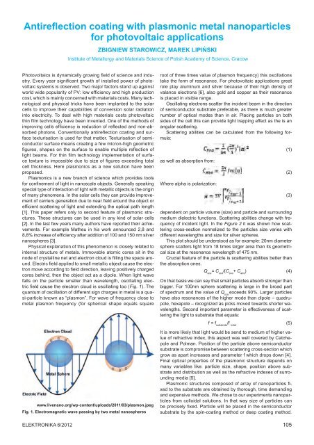
cores behind, <strong>the</strong>n <strong>the</strong> object act as a dipole. When light wave<br />
falls on <strong>the</strong> particle smaller than wavelength, oscillating electric<br />
field cause <strong>the</strong> electron cloud is oscillating too (Fig. 1). The<br />
quantum <strong>of</strong> oscillation <strong>of</strong> different sign charges in metal is a quasi-particle<br />
known as “plasmon”. For wave <strong>of</strong> frequency close to<br />
metal plasmon frequency (for spherical shape equals square<br />
www.livenano.org/wp-content/uploads/2011/03/plasmon.jpeg<br />
Fig. 1. Electromagnetic wave passing by two metal nanospheres<br />
root <strong>of</strong> three times value <strong>of</strong> plasmon frequency) this oscillations<br />
take <strong>the</strong> form <strong>of</strong> resonance. For photovoltaic applications great<br />
role play aluminum and silver because <strong>of</strong> <strong>the</strong>ir high density <strong>of</strong><br />
valance electrons [6], also gold and copper as <strong>the</strong>ir resonance<br />
is placed in visible range.<br />
Oscillating electrons scatter <strong>the</strong> incident beam in <strong>the</strong> direction<br />
<strong>of</strong> semiconductor substrate preferable, as <strong>the</strong>re is much greater<br />
number <strong>of</strong> optical modes than in air. Placing particles on both<br />
sides <strong>of</strong> <strong>the</strong> cell this can provide light trapping effect as <strong>the</strong> is an<br />
angular scattering.<br />
Scattering abilities can be calculated from <strong>the</strong> following formula:<br />
(1)<br />
as well as absorption from:<br />
(2)<br />
Where alpha is polarization:<br />
(3)<br />
dependent on particle volume (size) and particle and surrounding<br />
medium dielectric functions. Scattering abilities change with frequency<br />
<strong>of</strong> incident light. In <strong>the</strong> Figure 2 it was shown how scattering<br />
cross-section normalized to <strong>the</strong> particles size varies with<br />
different wavelengths and size for silver spheres.<br />
This plot should be understood as for example: 20nm diameter<br />
sphere scatters light from 18 times larger area than its geometrical<br />
size at <strong>the</strong> resonance wavelength <strong>of</strong> 475 nm.<br />
Crucial feature <strong>of</strong> <strong>the</strong> particle is scattering abilities better than<br />
<strong>the</strong> absorption ones.<br />
Q sca<br />
= C sca<br />
/(C sca<br />
+ C abs<br />
) (4)<br />
On that basis we can sey that small particles absorb stronger than<br />
bigger. For 100nm sphere scattering is large in <strong>the</strong> broad part<br />
<strong>of</strong> spectrum and <strong>the</strong> value <strong>of</strong> Q sca<br />
exceeds 90%. Larger particles<br />
have also resonances <strong>of</strong> <strong>the</strong> higher mode than dipole – quadrupole,<br />
hexapole – recognized as picks moved towards shorter wavelengths.<br />
Second important parameter is effectiveness <strong>of</strong> scattering<br />
<strong>the</strong> light to substrate that equals:<br />
f = f substrate<br />
/f total<br />
(5)<br />
It is more likely that light would be send to medium <strong>of</strong> higher value<br />
<strong>of</strong> refractive index, this aspect was well covered by Catchepole<br />
and Polman. Position <strong>of</strong> <strong>the</strong> particle above semiconductor<br />
substrate is compromise between scattering cross-section which<br />
grow as apart increases and parameter f which drops down [4].<br />
Final optical properties <strong>of</strong> <strong>the</strong> plasmonic structure depends on<br />
many variables like: particle size, shape, position above substrate<br />
and distribution as well as <strong>the</strong> refractive indexes <strong>of</strong> surrounding<br />
media [5].<br />
Plasmonic structures composed <strong>of</strong> array <strong>of</strong> nanoparticles fixed<br />
to <strong>the</strong> substrate are obtained by thorough, time demanding<br />
and expensive methods. We chose to our experiments nanoparticles<br />
from colloidal solutions. In that way size <strong>of</strong> particles can<br />
be precisely fixed. Particle will be placed in <strong>the</strong> semiconductor<br />
substrate by <strong>the</strong> spin-coating method or deep coating method.<br />
Elektronika 6/2012 105


