Proceedings of the European Summer School of Photovoltaics 4 â 7 ...
Proceedings of the European Summer School of Photovoltaics 4 â 7 ...
Proceedings of the European Summer School of Photovoltaics 4 â 7 ...
Create successful ePaper yourself
Turn your PDF publications into a flip-book with our unique Google optimized e-Paper software.
ature were simulated for solar cell with standard area (100 cm 2 )<br />
and thickness – 210 µm – Fig. 6.<br />
The mechanism <strong>of</strong> current flow in internal structure <strong>of</strong> cell is<br />
linked with temperature. Increase <strong>of</strong> temperature leads to linear<br />
fall <strong>of</strong> open circuit voltage and almost linear growth <strong>of</strong> short circuit<br />
current. Heating reduces <strong>the</strong> size <strong>of</strong> energy gap. The increase in<br />
<strong>the</strong> short-circuit current is caused by rising <strong>the</strong> absorbed photon<br />
current [5]. The heating has a destructive effect on <strong>the</strong> opencircuit<br />
voltage. Finally, <strong>the</strong> efficiency <strong>of</strong> solar cell is reduced<br />
accordingly. It is caused by reducing <strong>of</strong> conductivity. The rise <strong>of</strong><br />
temperature is also linked with high irradiation in areas with poor<br />
ventilation. It is very desirable to employ a good air circulation<br />
among PV systems.<br />
Summary<br />
The work referred to research on <strong>the</strong> factors which may contribute<br />
to decrease <strong>the</strong> efficiency <strong>of</strong> solar cells. Progressive degradation<br />
process for multi- and mono -crystalline solar cells was observed.<br />
Optical measurements showed that effective reflectance is worse<br />
for mc-Si than Cz-Si cells although <strong>the</strong>y were coated antireflective<br />
layer. It is caused generally by <strong>the</strong>ir heterogeneous structure. The<br />
process <strong>of</strong> texturization in case <strong>of</strong> Cz-Si improves <strong>the</strong>ir optical parameters.<br />
On <strong>the</strong> o<strong>the</strong>r hand it contributes to faster oxidation <strong>the</strong>ir<br />
surfaces. The process <strong>of</strong> obsolescence was finally corroborated by<br />
electrical measurements. The simulation <strong>of</strong> impact <strong>of</strong> heating showed,<br />
that its high values cause decrease <strong>of</strong> solar cells efficiency.<br />
References<br />
[1] Swatowska B., A. Stańco, P. Panek: The causes <strong>of</strong> silicon solar cells<br />
degradation. 35th International Microelectronics and Packaging IMAPS<br />
– IEEE CPMT 21–24 September, Gdańsk–Sobieszewo, Poland, 2011.<br />
[2] http://www.globalmarket.com/<br />
[3] Swatowska B., T. Stapiński, J. Chojnacki: Parameters <strong>of</strong> silicon solar<br />
cells in changeable external conditions. 23 International Conference <strong>of</strong><br />
IMAPS – CPMT IEEE 21–24 September, Pszczyna, Poland, 2009.<br />
[4] Strehlke S., S. Bastide, J. Guillet, C. Lévy – Clément: Design <strong>of</strong> porous<br />
silicon antireflection coatings for silicon solar cells. Materials<br />
Science and Engineering B69 – 70 (2000) 81–86.<br />
[5] Würfel P.: Physics <strong>of</strong> Solar Cells – From Principles to New Concepts.<br />
WILEY – VCH Verlag GmbH & Co. KGaA, Weinheim, Germany 2005.<br />
Low-ohmic contacts on <strong>the</strong> basis <strong>of</strong> silver nanopowder<br />
dedicated to photovoltaic cells<br />
Joanna Kalbarczyk, Marian Teodorczyk, Konrad Krzyżak, Grzegorz Gawlik,<br />
Mateusz Jarosz, Anna Młożniak<br />
Institute <strong>of</strong> Electronic Materials Technology, Warszawa<br />
Obtaining satisfactory parameters <strong>of</strong> solar cell is largely dependent<br />
on mastering <strong>the</strong> technique <strong>of</strong> producing contacts metal<br />
– semiconductor. The m-s contact can be strictly mechanical<br />
connection (e.g. trough contact electrode with semiconductor) as<br />
well as inseparable, integral connection. The m-s contacts may<br />
be regarded as ideal if <strong>the</strong>y generate no additional resistance for<br />
<strong>the</strong> current, do not react chemically with semiconductor material,<br />
do not change characterictics while changing illumination,<br />
temperature or value <strong>of</strong> applied electric filed and do not exhibit<br />
rectifying effects. Such contact can be described with Ohm’s law<br />
– its current-voltage characteristic is linear. It is obvious that ideal<br />
contacts do not exist, but <strong>the</strong> aim <strong>of</strong> <strong>the</strong> technology is to approach<br />
as close as possible to <strong>the</strong> imaginary ideal contact.<br />
To eliminate serious mistakes while creating ohmic contacts it<br />
is necessary to know <strong>the</strong> type <strong>of</strong> conduction. The material chosen<br />
for contacts should create impurity centers that comply with semiconductor’s<br />
type <strong>of</strong> conduction – it should contain donor impurities<br />
in case <strong>of</strong> contact with n – type semiconductor and acceptor<br />
impurities in case <strong>of</strong> p-type semiconductor.<br />
Except specified electrical properties <strong>the</strong>re are many o<strong>the</strong>r<br />
physicochemical properties (such as good <strong>the</strong>rmal conductivity,<br />
compatibility <strong>of</strong> metal and semiconductor coefficient <strong>of</strong> heat expansion,<br />
proper mechanical strength in different temperatures)<br />
that should characterize a useful m-s contact [1].<br />
In <strong>the</strong> following <strong>the</strong>sis, two methods <strong>of</strong> creating contacts will<br />
be presented.<br />
The first method is <strong>the</strong> cathode sputtering. The silicon base is<br />
subjected to high vacuum ion bombardment in inert atmosphere,<br />
<strong>the</strong>n silver layer is deposited. The method provides obtaining layer<br />
<strong>of</strong> high degree <strong>of</strong> purity.<br />
The second method <strong>of</strong> making contacts is applying <strong>the</strong> paste<br />
with silver nanopowder. The method is quite new and is an attempt<br />
<strong>of</strong> confrontation already well-known and bringing satisfactory<br />
effects in silver contact preparation procedure (sputtering)<br />
and a new method which uses up-to-date nanomaterial that may<br />
exhibit interesting properties for <strong>the</strong> technique <strong>of</strong> solar cells contact<br />
preparation [2, 4].<br />
82<br />
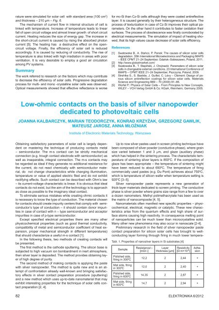
Tabl. 1. Properties <strong>of</strong> nanosilver layers in Si substrates [4]<br />
Sample<br />
Polished side,<br />
firing in 300 0 C<br />
Mat side, firing<br />
in 300 0 C<br />
Polished side,<br />
firing in 600 0 C<br />
Mat side, firing<br />
in 600 0 C<br />
Resistance/□<br />
[mΩ/□]<br />
Layer<br />
thickness [µm]<br />
Resistivity<br />
[Ω∙m×10 -8 ]<br />
Up to now silver pastes used in screen printing technique have<br />
been composed <strong>of</strong> silver powder (conductive phase), where grain<br />
size varied between 1 and 3 µm, and glaze (auxiliary phase)<br />
which has helped in <strong>the</strong> sintering process. The characteristic temperature<br />
<strong>of</strong> sintering silver layers is 850 0 C. If <strong>the</strong> composition <strong>of</strong><br />
glaze has been appropriate – <strong>the</strong> temperature <strong>of</strong> sintering might<br />
have been reduced to about 650 0 C. The temperature <strong>of</strong> firing<br />
commercially used pastes (e.g. Du Pont) achieves about 750 0 C,<br />
which is temperature <strong>of</strong> silicon wafer when temperature setting is<br />
920 0 C [3–5].<br />
Silver nanopowder paste represents a new generation <strong>of</strong><br />
thick-layer materials dedicated to screen printing. The conductive<br />
phase is silver powder where grains size range from a few to over<br />
a dozen nanometers. Methyl polimethacrylate has been used as<br />
<strong>the</strong> matrix <strong>of</strong> nanocomposite [4, 5].<br />
Nanomaterials <strong>of</strong>ten manifest new specific properties – physicochemical,<br />
electrical, magnetic or catalytic. These new characteristics<br />
arise from <strong>the</strong> quantum effects and high share <strong>of</strong> surface<br />
atoms causing high reactivity. In consequence melting point<br />
<strong>of</strong> nanoparticles can be much lower than microcrystalline solid.<br />
Many o<strong>the</strong>r new phenomena may also occur in nanoscale [2-4].<br />
Preliminary research in <strong>the</strong> field <strong>of</strong> silver nanopowder paste<br />
contact preparation for silicon solar cells has brought to wellconducting<br />
layer forming through firing in much lower tempera-<br />
Adhesion<br />
12,2 2 2,44 +<br />
12,0 2 2,40 +<br />
14,35 2 2,87 +<br />
14,7 2 2,94 +<br />
Elektronika 6/2012


