

Proceedings of the European Summer School of Photovoltaics 4 â 7 ...
Proceedings of the European Summer School of Photovoltaics 4 â 7 ...
Proceedings of the European Summer School of Photovoltaics 4 â 7 ...

You also want an ePaper? Increase the reach of your titles
YUMPU automatically turns print PDFs into web optimized ePapers that Google loves.
de are believed to change <strong>the</strong> ionizing potential <strong>of</strong> ITO (causing<br />
a rise in <strong>the</strong> work function <strong>of</strong> <strong>the</strong> latter, and so an increase in<br />
<strong>the</strong> built in potential) and as a result an increase in <strong>the</strong> open-circuit<br />
voltage [6]. O<strong>the</strong>rs think that <strong>the</strong>se layers block an electron<br />
transfer to <strong>the</strong> anode which causes an increase in j sc<br />
(short-circuit<br />
current), U oc<br />
and η (energy conversion efficiency) [7]. BCP is <strong>of</strong>ten<br />
used due to its exciton blocking ability and its positive effect on<br />
j sc<br />
, U oc<br />
and η [8]. It is also regarded as a protective interlayer that<br />
reduces damage caused to <strong>the</strong> active layer during cathode deposition<br />
process [9]. Dark j-V characteristics obtained for our cells<br />
show that introduction <strong>of</strong> BCP buffer layer has a noticeable impact<br />
on forward and reverse currents causing a significant rise in <strong>the</strong><br />
rectification ratio (RR) and decrease in series resistance (R s<br />
) <strong>of</strong><br />
a cell. We did not observe effect <strong>of</strong> anodic buffer layer on RR<br />
in <strong>the</strong> absence <strong>of</strong> BCP layer. However, cells incorporating both<br />
MoO 3<br />
and BCP interlayers had much higher rectification ratios<br />
than <strong>the</strong> ones with BCP buffer layer only. Results <strong>of</strong> our research<br />
show, that presence <strong>of</strong> MoO 3<br />
and BCP layers affects injection <strong>of</strong><br />
charge carriers at electrode/organic material interface and <strong>the</strong>ir<br />
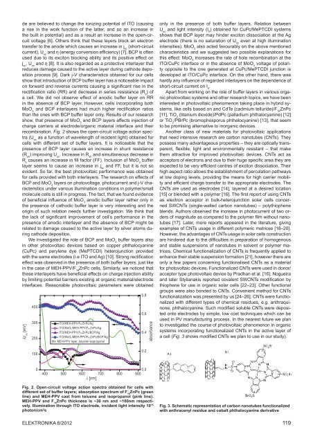
recombination. Fig. 2 shows <strong>the</strong> open-circuit voltage action spectra<br />
(U oc<br />
as a function <strong>of</strong> wavelength <strong>of</strong> incident light) obtained for<br />
cells with different set <strong>of</strong> buffer layers. It is noticeable that <strong>the</strong><br />
presence <strong>of</strong> BCP layer causes an increase in shunt resistance<br />
(R sh<br />
) improving U oc<br />
. Increase in R sh<br />
and simultaneous decrease in<br />
R s<br />
causes an increase in fill factor (FF). Inclusion <strong>of</strong> MoO 3<br />
buffer<br />
layer seems to cause an increase in j sc<br />
and FF, but it is not so<br />
evident. So far, <strong>the</strong> best photovoltaic performance was obtained<br />
for cells provided with both interlayers. The research on effects <strong>of</strong><br />
BCP and MoO 3<br />
layers on photovoltage, photocurrent and j-V characteristics<br />
under various illumination conditions in polymer/small<br />
molecule cells is still in progress. The fact, that we found evidence<br />
<strong>of</strong> beneficial influence <strong>of</strong> MoO 3<br />
anodic buffer layer ra<strong>the</strong>r only in<br />
<strong>the</strong> presence <strong>of</strong> cathodic buffer layer is very interesting and <strong>the</strong><br />
origin <strong>of</strong> such relation needs fur<strong>the</strong>r investigation. We think that<br />
<strong>the</strong> lack <strong>of</strong> significant improvement <strong>of</strong> cell’s performance in <strong>the</strong><br />
presence <strong>of</strong> anodic interlayer and <strong>the</strong> absence <strong>of</strong> BCP might be<br />
related to damage caused to <strong>the</strong> active layer by silver atoms during<br />
cathode deposition.<br />
We investigated <strong>the</strong> role <strong>of</strong> BCP and MoO 3<br />
buffer layers also<br />
in o<strong>the</strong>r photovoltaic devices based on copper phthalocyanine<br />
(CuPc) and perylene dye (MePTCDI) heterojunction provided<br />
with <strong>the</strong> same electrodes (i.e ITO and Ag) [10]. Strong rectification<br />
effect was observed in <strong>the</strong> presence <strong>of</strong> both buffer layers, just like<br />
in <strong>the</strong> case <strong>of</strong> MEH-PPV/F 16<br />
ZnPc cells. Similarly, we noticed that<br />
<strong>the</strong>se interlayers have beneficial effects on charge injection ability<br />
by limiting potential barriers existing at organic material/electrode<br />
interfaces. Reasonable photovoltaic parameters were obtained<br />
-U oc<br />
[mV]<br />
400<br />
300<br />
200<br />
ITO/MEH-PPV/F16 ZnPc/Ag<br />
ITO/MoO3 /MEH-PPV/F16 ZnPc/Ag<br />
ITO/MEH-PPV/F16 ZnPc/BCP/Ag<br />
ITO/MoO3/MEH-PPV/F16 ZnPc/BCP/Ag<br />
thin MEH-PPV layer, toluene+isopropanol<br />
0,8<br />
0,6<br />
0,4<br />
absorbance<br />
only in <strong>the</strong> presence <strong>of</strong> both buffer layers. Relation between<br />
U oc<br />
and light intensity (I 0<br />
) obtained for CuPc/MePTCDI systems<br />
shows that BCP layer may hinder exciton dissociation at <strong>the</strong> Ag<br />
electrode (<strong>the</strong>re is no saturation <strong>of</strong> U oc<br />
even at high illumination<br />
intensities). MoO 3<br />
also acted favourably on <strong>the</strong> above mentioned<br />
characteristics and we suggested two possible explanations for<br />
this effect: MoO 3<br />
increases <strong>the</strong> rate <strong>of</strong> hole recombination at <strong>the</strong><br />
ITO/CuPc interface or in <strong>the</strong> absence <strong>of</strong> MoO 3<br />
voltage <strong>of</strong> polarity<br />
opposite to <strong>the</strong> one generated at CuPc/MePTCDI junction is<br />
developed at ITO/CuPc interface. On <strong>the</strong> o<strong>the</strong>r hand, <strong>the</strong>re was<br />
hardly any influence <strong>of</strong> regarded interlayers on <strong>the</strong> dependence <strong>of</strong><br />
short-circuit current on I 0<br />
.<br />
Apart from working on <strong>the</strong> role <strong>of</strong> buffer layers in various organic<br />
photovoltaic systems and o<strong>the</strong>r research topics, we have been<br />
interested in photovoltaic phenomenon taking place in hybrid systems,<br />
like cells based on and CdTe (cadmium telluride)/F 16<br />
ZnPc<br />
[11], TiO 2<br />
(titanium dioxide)/PdPc (palladium phthalocyanine) [12]<br />
or TiO 2<br />
/PBrPc (bromophosporus phthalocyanine) [13], that seem<br />
to be promising alternative to inorganic devices.<br />
Ano<strong>the</strong>r class <strong>of</strong> new materials for photovoltaic applications<br />
that need intensive research are carbon nanotubes (CNTs). They<br />
possess many advantageous properties – <strong>the</strong>y are optically transparent,<br />
flexible, light and environmentally resistant – that make<br />
<strong>the</strong>m attractive for improved photovoltaic devices. CNTs act as<br />
acceptors <strong>of</strong> electrons and due to <strong>the</strong>ir huge specific area <strong>the</strong>y are<br />
expected to be very efficient centres <strong>of</strong> exciton dissociation. Their<br />
high aspect ratio allows <strong>the</strong> establishment <strong>of</strong> percolation pathways<br />
at low doping levels, providing <strong>the</strong> means for high carrier mobility<br />
and efficient charge transfer to <strong>the</strong> appropriate electrodes. The<br />
CNTs are used as electrodes [14], layered at a desired location<br />
[15] or blended with a polymer [16]. The first report <strong>of</strong> using CNTs<br />
as electron acceptor in bulk-heterojunction solar cells concerned<br />
SWCNTs (single-walled carbon nanotubes) – polythiophene<br />
blends. Authors observed <strong>the</strong> increase in photocurrent <strong>of</strong> two orders<br />
<strong>of</strong> magnitude as compared to <strong>the</strong> polymer film without nanotubes<br />
[17]. Later, more reports appeared in <strong>the</strong> literature, giving<br />
examples <strong>of</strong> CNTs usage in different polymeric matrices [18–20].<br />
However, <strong>the</strong> advantages <strong>of</strong> CNTs usage in solar cells construction<br />
are hindered due to <strong>the</strong> difficulties in preparation <strong>of</strong> homogenous<br />
and stable suspensions <strong>of</strong> nanotubes in solvent or polymer matrices.<br />
Chemical functionalization <strong>of</strong> CNTs is frequently applied to<br />
enhance <strong>the</strong>ir stable suspension formation [21], however <strong>the</strong>re are<br />
only a few papers concerning functionalised CNTs as a material<br />
for photovoltaic devices. Functionalized CNTs were used in donor/<br />
acceptor type photovoltaic device by Pradhan et al. [16]. Nogueira<br />
and later Stylianakis reported covalent SWCNTs modification by<br />
thiophene for use in organic solar cells [22–23]. O<strong>the</strong>r functional<br />
groups were also bonded to CNTs. Convenient method for CNTs<br />
functionalization was presented by us [24–26]. CNTs were functionalized<br />
with different types <strong>of</strong> chemical residues, e.g. anthraquinone,<br />
phthalocyanine. Such modified soluble CNTs were deposited<br />
onto electrodes by simple, low cost techniques which can be<br />
used in PV manufacturing process. In <strong>the</strong> nearest future we plan<br />
to investigated <strong>the</strong> course <strong>of</strong> photovoltaic phenomenon in organic<br />
systems incorporating functionalized CNTs in <strong>the</strong> active layer <strong>of</strong><br />
a cell (Fig. 3 shows modified CNTs we plan to use in our study).<br />
100<br />
0,2<br />
0<br />
0,0<br />
400 500 600 700 800 900<br />
λ [nm]<br />
Fig. 2. Open-circuit voltage action spectra obtained for cells with<br />
different set <strong>of</strong> buffer layers; absorption spectrum <strong>of</strong> F 16<br />
ZnPc (green<br />
line) and MEH-PPV cast from toluene and isopropanol (pink line).<br />
MEH-PPV and F 16<br />
ZnPc thickness is ~30 nm and ~100nm respectively.<br />
Illumination through ITO electrode, incident light intensity 10 15<br />
photon/cm 2 s<br />
Fig. 3. Schematic representation <strong>of</strong> carbon nanotubes functionalized<br />
with anthracenyl residue and cobalt phthalocyanine derivative<br />
Elektronika 6/2012 119


