

Proceedings of the European Summer School of Photovoltaics 4 â 7 ...
Proceedings of the European Summer School of Photovoltaics 4 â 7 ...
Proceedings of the European Summer School of Photovoltaics 4 â 7 ...

Create successful ePaper yourself
Turn your PDF publications into a flip-book with our unique Google optimized e-Paper software.
GaAsN as a photovoltaic material – photoelectrical<br />
characterization<br />
Paulina Kamyczek 1) , Ewa Placzek-Popko 1) , Piotr Biegański 1) , Eunika Zielony 1) ,<br />
Beata Sciana 2) , Marek TłaczaŁa 2)<br />
1)<br />
Institute <strong>of</strong> Physics, Wroclaw University <strong>of</strong> Technology<br />
2)<br />
Faculty <strong>of</strong> Microsystem Electronics and Photonics, Wroclaw University <strong>of</strong> Technology<br />
GaAsN and InGaAsN materials have attracted considerable attention<br />
due to <strong>the</strong>ir unique physical properties and wide range <strong>of</strong><br />
<strong>the</strong>ir possible application in optoelectronics, especially in infrared<br />
laser diodes for 1.3 and 1.55 mm [1, 2] and high efficiency<br />
multi-junction (MJ) solar sells [3, 4], where <strong>the</strong>se low-band-gap<br />
materials can, in principle, be used to efficiently collect <strong>the</strong> lowphoton-energy<br />
portion <strong>of</strong> <strong>the</strong> solar spectrum [4].<br />
In this paper <strong>the</strong> results <strong>of</strong> studies on <strong>the</strong> layers <strong>of</strong> GaAs 1-x<br />
N x<br />
grown on (100)-oriented Si-doped n-type GaAs substrates by atmospheric<br />
pressure metal organic vapour phase epitaxy APMO-<br />
VPE are presented. In <strong>the</strong> first step <strong>the</strong> layers <strong>of</strong> GaAs 1-x<br />
N x<br />
were<br />
characterized with <strong>the</strong> use <strong>of</strong> optical methods, <strong>the</strong>n Schottky diodes<br />
were realized and <strong>the</strong> rectifying properties <strong>of</strong> <strong>the</strong> diodes were<br />
studied with electrical methods. The diodes exhibit light-energy<br />
conversion effect. Basic parameters <strong>of</strong> <strong>the</strong> solar cells ( short-circuit<br />
current I sc<br />
, open circuit-voltage, V oc<br />
, and fill factor, FF) were<br />
determined. Obtained results confirm that <strong>the</strong> diodes are promising<br />
as efficient solar cells.<br />
Samples<br />
The investigated structures were grown on (100)-oriented Sidoped<br />
n-type GaAs substrates by APMOVPE with AIX200 R&D<br />
AIXTRON horizontal reactor. Trimethylgallium (TMGa), tertiarybutylhydrazine<br />
(TBHy) and arsine (AsH3) were used as <strong>the</strong> growth<br />
precursors. High purity hydrogen with <strong>the</strong> total flow rate <strong>of</strong><br />
9.6 l/min was employed as a carrier gas. The hydrogen flow rate<br />
through <strong>the</strong> saturator was changed during runs with TBHy - VH2/<br />
TBHy = 1500...2500 ml/min. Stable parameters were as follows:<br />
<strong>the</strong> growth temperature was Tg = 566°C , <strong>the</strong> arsine flow rate<br />
VAsH3 = 50 ml/min (for GaAsN) and 300 ml/min (for GaAs), <strong>the</strong><br />
organic source temperatures: TTMGa = −10°C, TTBHy = 30°C.<br />
The thickness <strong>of</strong> Si-doped n-type GaAs substrates was set to<br />
350 μm. Subsequently GaAs buffer layer <strong>of</strong> <strong>the</strong> thickness <strong>of</strong> 450<br />
nm was grown. The layer <strong>of</strong> 200...300 nm thick GaAs 1−x<br />
N x<br />
was<br />
grown on top <strong>of</strong> <strong>the</strong> buffer layer. Gold Schottky contacts <strong>of</strong> 0.5<br />
mm 2 area were prepared by electrolitography technique on <strong>the</strong><br />
front side <strong>of</strong> <strong>the</strong> GaAs 1−x<br />
N x<br />
layer. An AuGe served as <strong>the</strong> ohmic<br />
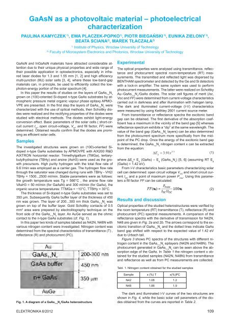
contact to <strong>the</strong> n-type GaAs substrates (cf. Fig. 1).<br />
In this paper two kinds <strong>of</strong> samples labeled as N42N, N48N with<br />
various nitrogen content were investigated. Nitrogen content was<br />
determined from <strong>the</strong> spectral characteristics <strong>of</strong> transmittance (T) ,<br />
reflectance (R) and photocurrent (PC).<br />
Experimental<br />
The optical properties were analysed using transmittance, reflectance<br />
and photocurrent spectral room-temperature (RT) measurements.<br />
The transmitted and reflected light was dispersed by<br />
BENTHAM spectrometer and detected by <strong>the</strong> Ge and Si detectors<br />
with a lock-in amplifier. The same system was used to perform<br />
photocurrent measurements. The latter were realized on Schottky<br />
Au–GaAs 1−x<br />
N x<br />
/GaAs diodes. The solar cell figures <strong>of</strong> merit (Isc,<br />
Voc and FF) were determined from current-voltage characteristics<br />
carried out in darkness and after illumination with halogen lamp.<br />
The dark and illuminated current-voltage (I-V) characteristics<br />
were measured by using Keithley 2601 current source meter.<br />
From transmittance or reflectance spectra <strong>the</strong> excitonic band<br />
gap can be obtained. The first derivative <strong>of</strong> <strong>the</strong> absorption coefficient<br />
has a maximum in <strong>the</strong> vicinity <strong>of</strong> <strong>the</strong> band gap [5] whereas<br />
reflectance spectrum exhibits a “dip” at <strong>the</strong> same wavelength. The<br />
value <strong>of</strong> <strong>the</strong> band gap (GaAs 1-x<br />
N x<br />
layers) can be also determined<br />
from <strong>the</strong> photocurrent spectrum more specifically from <strong>the</strong> midpoint<br />
<strong>of</strong> <strong>the</strong> PC drop. Once <strong>the</strong> energy <strong>of</strong> <strong>the</strong> excitonic band gap<br />
is determined, <strong>the</strong> GaAs 1-x<br />
N x<br />
nitrogen content x can be extracted<br />
from <strong>the</strong> equation:<br />
2/3<br />
∆ E = 3.91x<br />
(1)<br />
where ΔE g<br />
= E g<br />
(GaAs) – E g<br />
(GaAs 1x<br />
N x<br />
) [5, 6] (assuming RT E g<br />
(GaAs) = 1.42 eV).<br />
From I-V characteristics basic parameters characterizing solar<br />
cell can determined: open circuit voltage V OC<br />
and short circuit current<br />
I SC<br />
and a point <strong>of</strong> maximum power P max<br />
. Using this parameters<br />
a fill factor FF can be calculated:<br />
(2)<br />
Results and discussion<br />
g<br />
Optical properties <strong>of</strong> <strong>the</strong> studied heterostructures were verified by<br />
<strong>the</strong> room temperature (RT) transmittance (T), reflectance (R) and<br />
photocurrent (PC) spectral measurements. A comparison <strong>of</strong> <strong>the</strong><br />
reflectance spectra with <strong>the</strong> derivative <strong>of</strong> transmission for N42N,<br />
N48 are given in Fig. 2a and 2b. The arrows correspond to <strong>the</strong> excitonic<br />
transition <strong>of</strong> GaAs 1-x<br />
N x<br />
and <strong>the</strong> dotted lines indicate GaAs<br />
band gap shifted with respect to <strong>the</strong> expected value <strong>of</strong> 1.42 eV<br />
due to Urbach tail.<br />
Figure 3 shows PC spectra <strong>of</strong> <strong>the</strong> structures with different nitrogen<br />
content in <strong>the</strong> GaAs 1−x<br />
N x<br />
epilayers (N42N and N48N). The<br />
photocurrent generated in GaAs 1−x<br />
N x<br />
can be seen above <strong>the</strong> absorption<br />
edge <strong>of</strong> <strong>the</strong> GaAs. In Table 1 <strong>the</strong> nitrogen content x obtained<br />
for <strong>the</strong> studied samples (N42N, N48N) from transmittance<br />
and reflectance as well as from PC measurements are collected.<br />
Tabl. 1. Nitrogen content obtained for <strong>the</strong> studied samples<br />
Sample x (%) T x(%)PC<br />
N42 1.08 1.2<br />
N48 1.88 1.9<br />
Fig. 1. A diagram <strong>of</strong> a GaAs 1−x<br />
N x<br />
/GaAs heterostructure<br />
The dark and illuminated I-V curves <strong>of</strong> <strong>the</strong> two structures are<br />
shown in Fig. 4, while <strong>the</strong> basic solar cell parameters <strong>of</strong> <strong>the</strong> diodes<br />
obtained from <strong>the</strong> curves are reported in Table 2.<br />
Elektronika 6/2012 109


