

Proceedings of the European Summer School of Photovoltaics 4 â 7 ...
Proceedings of the European Summer School of Photovoltaics 4 â 7 ...
Proceedings of the European Summer School of Photovoltaics 4 â 7 ...

You also want an ePaper? Increase the reach of your titles
YUMPU automatically turns print PDFs into web optimized ePapers that Google loves.
Research achievements <strong>of</strong> <strong>the</strong> DSOD Lodz in <strong>the</strong> field<br />
<strong>of</strong> photovoltaics<br />
Katarzyna Znajdek, Maciej Sibiński<br />
Technical University <strong>of</strong> Lodz, Department <strong>of</strong> Semiconductor and Optoelectronic Devices<br />
The Department <strong>of</strong> Semiconductor and Optoelectronics Devices<br />
was established in 2008 as a part <strong>of</strong> <strong>the</strong> Faculty <strong>of</strong> Electrical,<br />
Electronic, Computer and Control Engineering at <strong>the</strong> Technical<br />
University <strong>of</strong> Lodz in Poland. The team <strong>of</strong> <strong>the</strong> DSOD Lodz consists<br />
<strong>of</strong> two pr<strong>of</strong>essors, two associate pr<strong>of</strong>essors, nine doctors,<br />
five PhD students and seven technical and administration employees.<br />
The Department’s research activities cover optoelectronic,<br />
micro- and nanoelectronic technologies, modeling and analysis <strong>of</strong><br />
electrical and <strong>the</strong>rmal phenomena in semiconductor devices, as<br />
well as designing and manufacturing <strong>of</strong> semiconductor devices,<br />
including solar cells. The main fields <strong>of</strong> <strong>the</strong> research interest are<br />
power semiconductor devices, high temperature electronics with<br />
emphasis on SiC technology, integrated intelligent systems, photonic<br />
systems and photovoltaic cells [1].<br />
Resources and technological base<br />
Both teaching and research activities are conducted in <strong>the</strong><br />
Department’s laboratories which enable investigation and experiments<br />
covering designing, manufacturing and testing <strong>of</strong> photovoltaic<br />
devices. Laboratories’ equipment base <strong>of</strong> <strong>the</strong> DSOD at TUL<br />
covers among o<strong>the</strong>rs:<br />
• Technological Centre <strong>of</strong> Microtechnology comprising Clean-<br />
Room laboratory, equipped with <strong>the</strong> facilities for fabrication<br />
and characterization <strong>of</strong> semiconductor or metal thin films, as<br />
well as for mapping <strong>of</strong> designed semiconductor structures.<br />
• Optoelectronics under <strong>the</strong> patronage <strong>of</strong> Corning Cable Systems<br />
Poland<br />
• Hybrid Systems Laboratory, equipped, inter alia, with <strong>the</strong><br />
pneumatic screen printer, <strong>the</strong> ball mill and <strong>the</strong> station for screen<br />
printing pastes preparation.<br />
• Photovoltaic Laboratory, fully equipped with an integrated<br />
measurement system that simulates standard test conditions<br />
STC, in accordance to <strong>the</strong> requirements <strong>of</strong> IEC 60904-1 and<br />
IEC 60904-3. The system includes C class solar simulator (in<br />
accordance to IEC 60904-9) with a silicon photodetector that<br />
controls <strong>the</strong> stability <strong>of</strong> <strong>the</strong> light source.<br />
• Specialized program SCAPS (Solar Cell Capacitance Simulator)<br />
for comprehensive simulations <strong>of</strong> solar cells dedicated to<br />
develop physical models and simulate new photovoltaic device<br />
structures.<br />
DSOD’s Laboratory <strong>of</strong> <strong>Photovoltaics</strong>, apart from technological<br />
and measuring equipment, possesses its own micro power solar<br />
plant <strong>of</strong> 2 kW p<br />
, consisted <strong>of</strong> four various types <strong>of</strong> photovoltaic arrays:<br />
– multicrystalline silicon: M-Si (6 modules <strong>of</strong> 115 W p<br />
each),<br />
– ribbon silicon: R-Si (6 modules <strong>of</strong> 110 W p<br />
each),<br />
– amorphous silicon: α-Si (6 modules <strong>of</strong> 64 W p<br />
each),<br />
– cooper indium diselenide: CIS (6 modules <strong>of</strong> 40 W p<br />
each).<br />
The installation is connected to <strong>the</strong> internal grid through Sunny<br />
Boy inverters, independently for each array type, which are<br />
<strong>the</strong>n attached toge<strong>the</strong>r by Sunny Boy Control Plus for data collection.<br />
All parameters <strong>of</strong> <strong>the</strong> PV plant are monitored and archived<br />
in <strong>the</strong> computer server located in <strong>the</strong> Laboratory. Moreover,<br />
<strong>the</strong>y can be observed in <strong>the</strong> real time conditions, by anyone (with<br />
no password or special access permission needed), via <strong>the</strong> PV<br />
Laboratory’s web site: http://www.fotowoltaika.dsod.pl [2]. Electricity<br />
produced by solar panels is used for <strong>the</strong> University internal<br />
power demands.<br />
134<br />
Research projects currently being realized<br />
Among seven currently running scientific projects in <strong>the</strong> Department<br />
<strong>of</strong> Semiconductor and Optoelectronics Devices, two <strong>of</strong> <strong>the</strong>m<br />
are being realized in <strong>the</strong> field <strong>of</strong> photovoltaics. One <strong>of</strong> <strong>the</strong>m is<br />
Polish research project granted by <strong>the</strong> National Science Centre<br />
within <strong>the</strong> program Opus (general grant). The o<strong>the</strong>r one is a project<br />
supporting international cooperation granted by <strong>the</strong> Ministry <strong>of</strong><br />
Science and Higher Education under <strong>the</strong> Polonium program.<br />
Opus: Transparent emitter electrode for PV<br />
applications based on carbon nanotubes<br />
This project is being realized by DSOD Lodz as a leader, in cooperation<br />
with two o<strong>the</strong>r Polish research centers, which are: Institute<br />
<strong>of</strong> Electronic Materials Technology <strong>of</strong> <strong>the</strong> Warsaw University<br />
<strong>of</strong> Technology and Institute <strong>of</strong> Fluid-Flow Machinery <strong>of</strong> <strong>the</strong> Polish<br />
Academy <strong>of</strong> Sciences. It has been granted by <strong>the</strong> National Science<br />
Centre for two years, from January 2012 to December 2013.<br />
The aim <strong>of</strong> <strong>the</strong> project is to manufacture transparent conductive<br />
layers, based on carbon nanotubes (CNT), and apply <strong>the</strong>m<br />
as front electrodes <strong>of</strong> various types solar cells. Obtaining thin,<br />
flexible transparent layers is to be achieved by using low-cost manufacturing<br />
techniques, such as screen printing, and by utilizing<br />
crude, easily available nanotube material with organic media.<br />
Created layers would replace currently used conductive oxides,<br />
such as ITO or ZnO: Al. Their application as transparent contacts<br />
in photovoltaic structures would eliminate certain disadvantages<br />
<strong>of</strong> previously used electrodes, such as fracturing in flexible photovoltaic<br />
structures. Additionally, exploration possibilities <strong>of</strong> new<br />
devices, manufacturing in roll-to-roll process, with no use <strong>of</strong> expensive<br />
vacuum technology, is planned [3].<br />
The following research work are scheduled in <strong>the</strong> project:<br />
– Preparation <strong>of</strong> carbon nanotube based suspensions <strong>of</strong> various<br />
composition and percentage, testing <strong>the</strong>ir properties and developing<br />
techniques, allowing to deposit controlled layer on test<br />
substrates. Simultaneously, a number <strong>of</strong> selected conductive<br />
oxide samples, including indium tin oxide ITO, ZnO 2<br />
and ZnO:<br />
Al, is expected to be manufactured, in order to compare optoelectronic<br />
and mechanical properties <strong>of</strong> new and traditional<br />
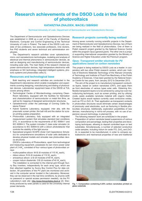
Fig. 1. Composition containing 0.25% carbon nanotubes printed on<br />
glass substrate<br />
Elektronika 6/2012


