

Proceedings of the European Summer School of Photovoltaics 4 â 7 ...
Proceedings of the European Summer School of Photovoltaics 4 â 7 ...
Proceedings of the European Summer School of Photovoltaics 4 â 7 ...

You also want an ePaper? Increase the reach of your titles
YUMPU automatically turns print PDFs into web optimized ePapers that Google loves.
I[µA/cm 2 ]<br />
15<br />
10<br />
5<br />
0<br />
-5<br />
-10<br />
I[µA/cm 2 ]<br />
15<br />
10<br />
5<br />
0<br />
-5<br />
-10<br />
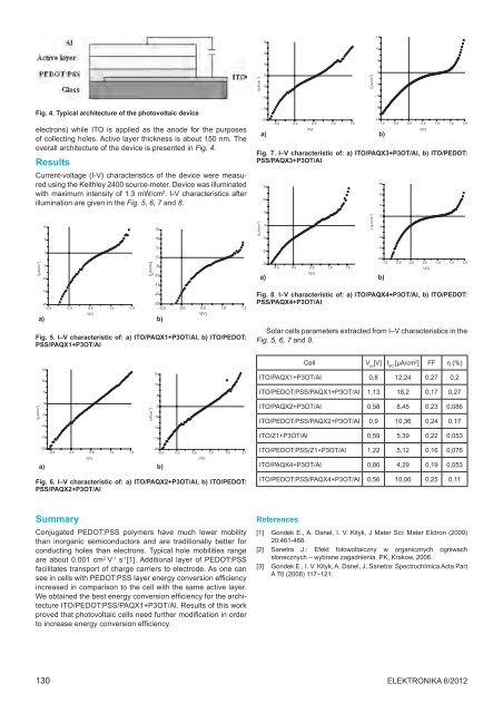
Fig. 4. Typical architecture <strong>of</strong> <strong>the</strong> photovoltaic device<br />
electrons) while ITO is applied as <strong>the</strong> anode for <strong>the</strong> purposes<br />
<strong>of</strong> collecting holes. Active layer thickness is about 150 nm. The<br />
overall architecture <strong>of</strong> <strong>the</strong> device is presented in Fig. 4.<br />
Results<br />
Current-voltage (I-V) characteristics <strong>of</strong> <strong>the</strong> device were measured<br />
using <strong>the</strong> Keithley 2400 source-meter. Device was illuminated<br />
with maximum intensity <strong>of</strong> 1.3 mW/cm 2 . I-V characteristics after<br />
illumination are given in <strong>the</strong> Fig. 5, 6, 7 and 8.<br />
-15<br />
-20<br />
-0,5 0,0 0,5 1,0 1,5<br />
V[V]<br />
a) b)<br />
Fig. 7. I–V characteristic <strong>of</strong>: a) ITO/PAQX3+P3OT/Al, b) ITO/PEDOT:<br />
PSS/PAQX3+P3OT/Al<br />
30<br />
20<br />
-15<br />
-20<br />
-1,0 -0,5 0,0 0,5 1,0 1,5 2,0<br />
15<br />
10<br />
5<br />
V[V]<br />
10<br />
5<br />
15<br />
10<br />
I[µA/cm 2 ]<br />
10<br />
0<br />
-10<br />
I [µΑ/cm 2 ]<br />
0<br />
-5<br />
-10<br />
I[µA/cm 2 ]<br />
0<br />
-5<br />
-10<br />
-15<br />
-20<br />
-0,5 0,0 0,5 1,0 1,5<br />
V[V]<br />
a) b)<br />
-25<br />
-0,5 0,0 0,5 1,0 1,5<br />
V[V]<br />
Fig. 5. I–V characteristic <strong>of</strong>: a) ITO/PAQX1+P3OT/Al, b) ITO/PEDOT:<br />
PSS/PAQX1+P3OT/Al<br />
I[ µ A/cm2]<br />
5<br />
0<br />
-5<br />
-10<br />
-15<br />
-20<br />
-20<br />
-30<br />
-0,5 0,0 0,5 1,0 1,5<br />
V[V]<br />
a) b)<br />
Fig. 8. I–V characteristic <strong>of</strong>: a) ITO/PAQX4+P3OT/Al, b) ITO/PEDOT:<br />
PSS/PAQX4+P3OT/Al<br />
Solar cells parameters extracted from I–V characteristics in <strong>the</strong><br />
Fig. 5, 6, 7 and 8.<br />
-15<br />
-20<br />
-1,0 -0,5 0,0 0,5 1,0 1,5 2,0<br />
U[V]<br />
I[µA/cm 2 ]<br />
15<br />
10<br />
5<br />
0<br />
-5<br />
-10<br />
-15<br />
IµA/cm 2 ]<br />
15<br />
10<br />
5<br />
0<br />
-5<br />
-10<br />
-15<br />
Cell V oc<br />
[V] I SC<br />
[μA/cm 2 ] FF η (%)<br />
ITO/PAQX1+P3OT/Al 0,8 12,24 0,27 0,2<br />
ITO/PEDOT:PSS/PAQX1+P3OT/Al 1,13 18,2 0,17 0,27<br />
ITO/PAQX2+P3OT/Al 0,58 8,45 0,23 0,086<br />
ITO/PEDOT:PSS/PAQX2+P3OT/Al 0,9 10,36 0,24 0,17<br />
ITO/Z1+P3OT/Al 0,59 5,39 0,22 0,053<br />
-20<br />
-0,5 0,0 0,5 1,0 1,5<br />
V[V]<br />
a) b)<br />
-20<br />
-0,5 0,0 0,5 1,0 1,5 2,0<br />
Fig. 6. I–V characteristic <strong>of</strong>: a) ITO/PAQX2+P3OT/Al, b) ITO/PEDOT:<br />
PSS/PAQX2+P3OT/Al<br />
V[V]<br />
ITO/PEDOT:PSS/Z1+P3OT/Al 1,22 5,12 0,16 0,076<br />
ITO/PAQX4+P3OT/Al 0,86 4,29 0,19 0,053<br />
ITO/PEDOT:PSS/PAQX4+P3OT/Al 0,56 10,06 0,25 0,11<br />
Summary<br />
Conjugated PEDOT:PSS polymers have much lower mobility<br />
than inorganic semiconductors and are traditionally better for<br />
conducting holes than electrons. Typical hole mobilities range<br />
are about 0.001 cm 2 V -1 s -1 [1]. Additional layer <strong>of</strong> PEDOT:PSS<br />
facilitates transport <strong>of</strong> charge carriers to electrode. As one can<br />
see in cells with PEDOT:PSS layer energy conversion efficiency<br />
increased in comparison to <strong>the</strong> cell with <strong>the</strong> same active layer.<br />
We obtained <strong>the</strong> best energy conversion efficiency for <strong>the</strong> architecture<br />
ITO/PEDOT:PSS/PAQX1+P3OT/Al. Results <strong>of</strong> this work<br />
proved that photovoltaic cells need fur<strong>the</strong>r modification in order<br />
to increase energy conversion efficiency.<br />
References<br />
[1] Gondek E., A. Danel, I. V. Kityk, J Mater Sci: Mater Elctron (2009)<br />
20:461-468.<br />
[2] Sanetra J.: Efekt fotowoltaiczny w organicznych ogniwach<br />
słonecznych – wybrane zagadnienia. PK, Krakow, 2006.<br />
[3] Gondek E., I. V. Kityk, A. Danel, J. Sanetra: SpectrochImica Acta Part<br />
A 70 (2008) 117–121.<br />
130<br />
Elektronika 6/2012


