

Proceedings of the European Summer School of Photovoltaics 4 â 7 ...
Proceedings of the European Summer School of Photovoltaics 4 â 7 ...
Proceedings of the European Summer School of Photovoltaics 4 â 7 ...

Create successful ePaper yourself
Turn your PDF publications into a flip-book with our unique Google optimized e-Paper software.
Tab. 2. The roughness parameters <strong>of</strong> <strong>the</strong> polyoxadiazoles thin films in <strong>the</strong><br />
program carried out XEI’s Park System<br />
Spin speed [rev/min] Max height [nm] R a<br />
[nm] R q<br />
[nm]<br />
1000 33,728 10,634 14,447<br />
2000 46,776 5,276 10,999<br />
3000 43,010 4,773 8,393<br />
Where: Rq – <strong>the</strong> root-mean-squared roughness. It is <strong>the</strong> standard deviation<br />
<strong>of</strong> <strong>the</strong> height value, Ra – <strong>the</strong> roughness average, Max height – a maximum<br />
height.<br />
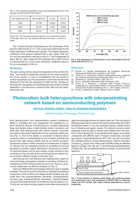
Fig. 6. shows <strong>the</strong> plot <strong>of</strong> absorbance on <strong>the</strong> wavelength <strong>of</strong> <strong>the</strong><br />
polymer DDE-Per-6F (2:1:1). The curves were determined for <strong>the</strong><br />
layers deposited at different spin speeds. The largest absorption<br />
coefficient <strong>of</strong> <strong>the</strong> polymer obtained with a spin speed 1000 rev/<br />
min and <strong>the</strong> absorbance reached a value <strong>of</strong> 1.3 at a wavelength <strong>of</strong><br />
about 380 nm. Spin coated thin film obtained with a 2000 rev/min<br />
is characterized by a much lower absorption coefficient equal to<br />
0.8 at a wavelength <strong>of</strong> 350 nm.<br />
Summary<br />
The spin coating method allows <strong>the</strong> deposition <strong>of</strong> <strong>the</strong> uniform thin<br />
films. The process is dependent primarily on <strong>the</strong> correct preparation<br />
<strong>of</strong> <strong>the</strong> solution. In view <strong>of</strong> consideration both <strong>the</strong> results <strong>of</strong><br />
surface topography and <strong>the</strong> absorbance <strong>of</strong> <strong>the</strong> best results were<br />
obtained for <strong>the</strong> thin film deposited at 3000 rev/min. Studies on<br />
<strong>the</strong> polymers conjugated are interesting because <strong>of</strong> <strong>the</strong>ir possible<br />
application in <strong>the</strong> structure <strong>of</strong> polymer solar cells and dye sensitized<br />
solar cells.<br />
Fig. 6. The dependence <strong>of</strong> absorbance on <strong>the</strong> wavelength <strong>of</strong> <strong>the</strong> polymer<br />
DDE-Per-6F (2:1:1)<br />
References<br />
[1] Drozdov N.: Ogniwa fotowoltaiczne dla energetyki słonecznej.<br />
Wydawnictwo Politechniki Lubelskiej, Lublin 2006.<br />
[2] Torbicz W., D. Pijanowska: Polimery elektroprzewodzące w elektronice<br />
i analityce biochemicznej. Elektronika 2009, nr 6, s. 36–43.<br />
[3] Shirakawa H.: Syn<strong>the</strong>tic Metals. 1995, 69, 3–8.<br />
[4] Gruin I.: Materiały polimerowe. PWN, Warszawa, 2003.<br />
[5] Schulz B., Y. Kaminorz; L. Brehmer: New Aromatic Poly(l,3,4-<br />
oxadiazole)s for Light Emitting Diodes. University Potsdam, Institute<br />
<strong>of</strong> Solid State Physics Kantstrasse 55, D – 14513 Teltow, Germany.<br />
[6] Poroń A.: Syntetyczne metale. Wiedza i Życie nr 2/2001.<br />
Photovoltaic bulk heterojunctions with interpenetrating<br />
network based on semiconducting polymers<br />
Michał Modzelewski, Ewa Klugmann-Radziemska<br />
Gdańsk University <strong>of</strong> Technology, Chemical Faculty<br />
Bulk heterojunctions with interpenetrating network architecture<br />
(BHS) is nowadays <strong>the</strong> most prospective one exploited for organic<br />
electronic devices manufacturing as it enables fabricating<br />
large and flexible areas <strong>of</strong> light-emitting diodes, transistors and<br />
solar cells. Bulk heterojunction with internal network <strong>of</strong> percolation<br />
paths is intermixed spatial blend <strong>of</strong> two physically stable phases<br />
(Fig. 1). One <strong>of</strong> <strong>the</strong> phases is composed <strong>of</strong> electron-donor<br />
compound which is characterized by low ionization potential and<br />
second with high electron affinity acts as an electron-acceptor.<br />
Exceptional position <strong>of</strong> BHS amongst all architectures <strong>of</strong> organic<br />
PV devices can be explained primarily by possibility <strong>of</strong> low-cost<br />
deposition <strong>of</strong> soluble organic photoactive compounds by means<br />
<strong>of</strong> novel techniques such as spin-coating, screen printing or doctor<br />
blading on <strong>the</strong> one side and by achieving internal network within<br />
an exciton diffusion length on <strong>the</strong> o<strong>the</strong>r side.<br />
Until that day <strong>the</strong> most effective bulk heterojunction based on<br />
semiconducting (conjugated) polymers is structure <strong>of</strong> Poly(3-hexyltiophene)<br />
(P3HT) acting as electron donor an Phenyl-C 60<br />
-butyric<br />
acid methyl ester as electron acceptor [1] (Fig. 2).<br />
There are different BHJ technologies referred to type <strong>of</strong> applied<br />
materials. The common part for all <strong>of</strong> <strong>the</strong>m is solubility <strong>of</strong> constituent<br />
compounds. As far as BHJs are charge transfer systems one may<br />
divide <strong>the</strong>m into polymer/fullerene derivatives, polymer/polymer,<br />
low-band gap polymers/fullerene derivatives, polymer/inorganic<br />
compound and polymer/oxide. All mentioned may be doped or not.<br />
To find our own place amongst organic photovoltaic we decided to<br />
122<br />
apply low-band gap polymer for organic solar cell. The main goal <strong>of</strong><br />
following paper was to construct an organic photovoltaic cell in BHJ<br />
architecture based on very low band gap polymer, soluble derivative<br />
<strong>of</strong> fullerene and organic dopant. To construct a junction which<br />
potentially would be able to harvest solar radiation from <strong>the</strong> spectrum<br />
<strong>of</strong> near infrared (Fig. 3) we selected three organic and soluble<br />
compounds with different type <strong>of</strong> induced conductivity: low-band<br />
gap polymer poly(indenefluorene) (PIF) (Fig. 4a) with low ionization<br />
potential acting as a base electron-donor, fullerene derivative<br />
<strong>of</strong> phenyl-C 60<br />
-butyric acid methyl ester (PCBM) acting as effective<br />
electron acceptor (Fig. 2b) and 7,7,8,8-tetracyanoquinodimethane<br />
(TCNQ) (Fig. 4b) as additional electron-acceptor <strong>of</strong> photoinduced<br />
electrons.<br />
Low iron glass<br />
PEDOT:PSS<br />
Light<br />
Donor:acceptor intermixed blend<br />
Indium Tin Oxide<br />
Metal cathode<br />
Fig. 1. Cross-section <strong>of</strong> organic photovoltaic cell containing blend<br />
as a photoactive layer and composed <strong>of</strong> PEDOT:PSS on substrate<br />
made from ITO (anode) with metal cathode deposited by vacuum<br />
evaporator<br />
Elektronika 6/2012


