

Proceedings of the European Summer School of Photovoltaics 4 â 7 ...
Proceedings of the European Summer School of Photovoltaics 4 â 7 ...
Proceedings of the European Summer School of Photovoltaics 4 â 7 ...

Create successful ePaper yourself
Turn your PDF publications into a flip-book with our unique Google optimized e-Paper software.
tures in comparison to so far used pastes. Obtained resistance<br />
results for paste firing in 300 and 600 0 C are similar. Resistivity<br />
– firing temperature relationship has shown that already from<br />
250 0 C layers exhibit very good electric conductivity which insignificantly<br />
fluctuates with <strong>the</strong> firing temperature escalation. Results<br />
<strong>of</strong> layer resistance after firing in different conditions have<br />
been shown in Table 1 [4].<br />
The main advantages <strong>of</strong> silver nanopastes is that <strong>the</strong>y do not<br />
contain <strong>the</strong> glaze phase, which impaired electric conduction <strong>of</strong><br />
<strong>the</strong> layer, and <strong>the</strong> possibility <strong>of</strong> firing in lower temperatures. Obtained<br />
results demonstrates that layers made from pastes with<br />
silver nanopowder can be used as ohmic contacts for silicon solar<br />
cells [3].<br />
Experiment<br />
The aim <strong>of</strong> <strong>the</strong> first stage <strong>of</strong> research was to determine electrical<br />
properties <strong>of</strong> contacts made with sputtering method. Such contacts<br />
have been already used to investigate electrical and optical<br />
properties <strong>of</strong> edge-illuminated silicon solar cells and enabled to<br />
acquire repeatable, satisfactory results. Because <strong>of</strong> that <strong>the</strong> sputtering-method-made<br />
contacts have been acknowledged as a good<br />
comparative base for new type <strong>of</strong> silver nanopowder contacts.<br />
Resistance has been measured with two point probe connected<br />
with multimeter. The silver layers have been applied trough<br />
a mask and three values <strong>of</strong> resistance have been measured. The<br />
scheme <strong>of</strong> <strong>the</strong> sample with applied contacts and measurement<br />
points have been shown on Fig. 1.<br />
a)<br />
b)<br />
c)<br />
Fig. 1. The scheme <strong>of</strong> measurement sample with “sputtered” contacts;<br />
R1, R2, R3 – values <strong>of</strong> resistance between marked silver layers<br />
The resistance measurement has to be made with comparative<br />
method, because obtained values do not define directly single<br />
contact resistance, but contain also resistances <strong>of</strong> particular meter<br />
circuit elements and foundation material.<br />
After sputtering process, <strong>the</strong> layer has been firing in RTP AG<br />
Heatpulse system (Rapid Thermal Processing) in nitrogen atmosphere.<br />
The parameters – temperature and time – <strong>of</strong> contacts’<br />
firing have been varied to optimize <strong>the</strong> process.<br />
Resistances have been measured both directly after sputtering<br />
process and after <strong>the</strong> firing in different conditions. It enabled<br />
to determine <strong>the</strong> optimum processing parameters <strong>of</strong> <strong>the</strong> contact<br />
preparing.<br />
Analogically experimental work concerning applying nanosilver<br />
pastes has been barely begun. The screen printer and suitable<br />
masks has been prepared for applying <strong>the</strong> paste on basic silicon<br />
wafers. Experimental research schedule has been established.<br />
Results <strong>of</strong> sputtering-method-made contacts<br />
The results for <strong>the</strong>se method have been elaborated for three kinds<br />
<strong>of</strong> base material: silicon wafer doped with boron (B), silicon wafer<br />
doped with phosphorus (P) and silicon wafer doped with antimony<br />
(Sb). The results are shown on graphs below. Resistances R1, R2<br />
and R3 are resistances between points as shown on Fig. 1.<br />
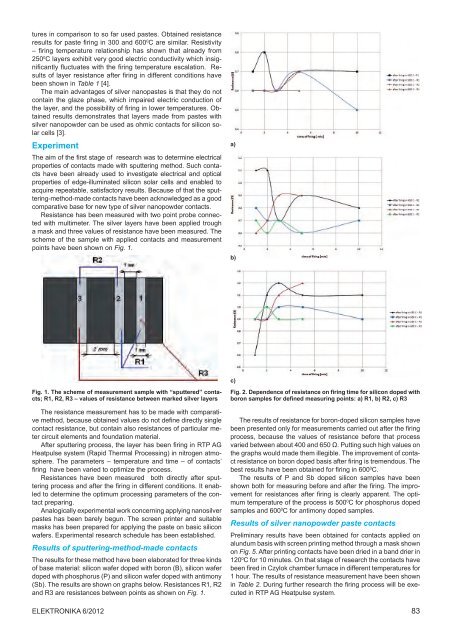
Fig. 2. Dependence <strong>of</strong> resistance on firing time for silicon doped with<br />
boron samples for defined measuring points: a) R1, b) R2, c) R3<br />
The results <strong>of</strong> resistance for boron-doped silicon samples have<br />
been presented only for measurements carried out after <strong>the</strong> firing<br />
process, because <strong>the</strong> values <strong>of</strong> resistance before that process<br />
varied between about 400 and 650 Ω. Putting such high values on<br />
<strong>the</strong> graphs would made <strong>the</strong>m illegible. The improvement <strong>of</strong> contact<br />
resistance on boron doped basis after firing is tremendous. The<br />
best results have been obtained for firing in 600 0 C.<br />
The results <strong>of</strong> P and Sb doped silicon samples have been<br />
shown both for measuring before and after <strong>the</strong> firing. The improvement<br />
for resistances after firing is clearly apparent. The optimum<br />
temperature <strong>of</strong> <strong>the</strong> process is 500 0 C for phosphorus doped<br />
samples and 600 0 C for antimony doped samples.<br />
Results <strong>of</strong> silver nanopowder paste contacts<br />
Preliminary results have been obtained for contacts applied on<br />
alundum basis with screen printing method through a mask shown<br />
on Fig. 5. After printing contacts have been dried in a band drier in<br />
120 0 C for 10 minutes. On that stage <strong>of</strong> research <strong>the</strong> contacts have<br />
been fired in Czylok chamber furnace in different temperatures for<br />
1 hour. The results <strong>of</strong> resistance measurement have been shown<br />
in Table 2. During fur<strong>the</strong>r research <strong>the</strong> firing process will be executed<br />
in RTP AG Heatpulse system.<br />
Elektronika 6/2012 83


