

Proceedings of the European Summer School of Photovoltaics 4 â 7 ...
Proceedings of the European Summer School of Photovoltaics 4 â 7 ...
Proceedings of the European Summer School of Photovoltaics 4 â 7 ...

You also want an ePaper? Increase the reach of your titles
YUMPU automatically turns print PDFs into web optimized ePapers that Google loves.
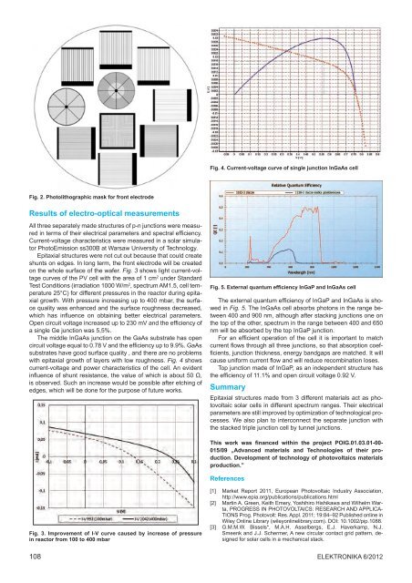
Fig. 4. Current-voltage curve <strong>of</strong> single junction InGaAs cell<br />
Fig. 2. Photolithographic mask for front electrode<br />
Results <strong>of</strong> electro-optical measurements<br />
All three separately made structures <strong>of</strong> p-n junctions were measured<br />
in terms <strong>of</strong> <strong>the</strong>ir electrical parameters and spectral efficiency.<br />
Current-voltage characteristics were measured in a solar simulator<br />
PhotoEmission ss300B at Warsaw University <strong>of</strong> Technology.<br />
Epitaxial structures were not cut out because that could create<br />
shunts on edges. In long term, <strong>the</strong> front electrode will be created<br />
on <strong>the</strong> whole surface <strong>of</strong> <strong>the</strong> wafer. Fig. 3 shows light current-voltage<br />
curves <strong>of</strong> <strong>the</strong> PV cell with <strong>the</strong> area <strong>of</strong> 1 cm 2 under Standard<br />
Test Conditions (irradiation 1000 W/m 2 , spectrum AM1.5, cell temperature<br />
25°C) for different pressures in <strong>the</strong> reactor during epitaxial<br />
growth. With pressure increasing up to 400 mbar, <strong>the</strong> surface<br />
quality was enhanced and <strong>the</strong> surface roughness decreased,<br />
which has influence on obtaining better electrical parameters.<br />
Open circuit voltage increased up to 230 mV and <strong>the</strong> efficiency <strong>of</strong><br />
a single Ge junction was 5,5%.<br />
The middle InGaAs junction on <strong>the</strong> GaAs substrate has open<br />
circuit voltage equal to 0.78 V and <strong>the</strong> efficiency up to 9.9%. GaAs<br />
substrates have good surface quality , and <strong>the</strong>re are no problems<br />
with epitaxial growth <strong>of</strong> layers with low roughness. Fig. 4 shows<br />
current-voltage and power characteristics <strong>of</strong> <strong>the</strong> cell. An evident<br />
influence <strong>of</strong> shunt resistance, <strong>the</strong> value <strong>of</strong> which is about 50 Ω,<br />
is observed. Such an increase would be possible after etching <strong>of</strong><br />
edges, which will be done for <strong>the</strong> purpose <strong>of</strong> future works.<br />
Fig. 5. External quantum efficiency InGaP and InGaAs cell<br />
The external quantum efficiency <strong>of</strong> InGaP and InGaAs is showed<br />
in Fig. 5. The InGaAs cell absorbs photons in <strong>the</strong> range between<br />
400 and 900 nm, although after stacking junctions one on<br />
<strong>the</strong> top <strong>of</strong> <strong>the</strong> o<strong>the</strong>r, spectrum in <strong>the</strong> range between 400 and 650<br />
nm will be absorbed by <strong>the</strong> top InGaP junction.<br />
For an efficient operation <strong>of</strong> <strong>the</strong> cell it is important to match<br />
current flows through all three junctions, so that absorption coefficients,<br />
junction thickness, energy bandgaps are matched. It will<br />
cause uniform current flow and will reduce recombination loses.<br />
Top junction made <strong>of</strong> InGaP, as an independent structure has<br />
<strong>the</strong> efficiency <strong>of</strong> 11.1% and open circuit voltage 0.92 V.<br />
Summary<br />
Epitaxial structures made from 3 different materials act as photovoltaic<br />
solar cells in different spectrum ranges. Their electrical<br />
parameters are still improved by optimization <strong>of</strong> technological processes.<br />
We also plan to interconnect <strong>the</strong> separate junction with<br />
<strong>the</strong> stacked triple junction cell by tunnel junctions.<br />
This work was financed within <strong>the</strong> project POIG.01.03.01-00-<br />
015/09 „Advanced materials and Technologies <strong>of</strong> <strong>the</strong>ir production.<br />
Development <strong>of</strong> technology <strong>of</strong> photovoltaics materials<br />
production.”<br />
References<br />
Fig. 3. Improvement <strong>of</strong> I-V curve caused by increase <strong>of</strong> pressure<br />
in reactor from 100 to 400 mbar<br />
[1] Market Report 2011, <strong>European</strong> Photovoltaic Industry Association,<br />
http://www.epia.org/publications/publications.html<br />
[2] Martin A. Green, Keith Emery, Yoshihiro Hishikawa and Wilhelm Warta,<br />
PROGRESS IN PHOTOVOLTAICS: RESEARCH AND APPLICA-<br />
TIONS Prog. Photovolt: Res. Appl. 2011; 19:84–92 Published online in<br />
Wiley Online Library (wileyonlinelibrary.com). DOI: 10.1002/pip.1088.<br />
[3] G.M.M.W. Bissels*, M.A.H. Asselbergs, E.J. Haverkamp, N.J.<br />
Smeenk and J.J. Schermer, A new circular contact grid pattern, designed<br />
for solar cells in a mechanical stack.<br />
108<br />
Elektronika 6/2012


