Proceedings of the European Summer School of Photovoltaics 4 â 7 ...
Proceedings of the European Summer School of Photovoltaics 4 â 7 ...
Proceedings of the European Summer School of Photovoltaics 4 â 7 ...
Create successful ePaper yourself
Turn your PDF publications into a flip-book with our unique Google optimized e-Paper software.
Optical and electrical parameters <strong>of</strong> thin oxide films based on TiO 2<br />
Thin film [% at.]<br />
T 550<br />
[%]<br />
λ cut<strong>of</strong>f<br />
[nm]<br />
ρ 300K<br />
[Ω cm]<br />
S<br />
[mV/K]<br />
TiO 2<br />
83 338 1·10 11 – –<br />
TiO 2<br />
:(5.5 Pd) 50 370 9.6·10 2 -11<br />
Ti-V oxides (3.0 V) 73 381 2.7·10 5 -200<br />
Ti-V oxides (23.0 V) 73 430 5,6·10 2 -20 n type<br />
TiO 2<br />
:(0.9 Eu, 5.8 Pd) 35 450 2.2·10 -1 -90<br />
TiO 2<br />
:(10.2 V, 6.9 Pd) 40 400 1.5 -410<br />
Ti-V oxides (19.0 V) 73 380 8·10 4 +685<br />
TiO 2<br />
:(15.8 Co, 6.9 Pd) 29 * 560 3.5·10 3 +77.5 p type<br />
TiO 2<br />
:(0.6 Tb, 9.0 Pd) 22 * 510 1·10 5 +120<br />
* average transmission determined at <strong>the</strong> wavelength λ=650 nm<br />
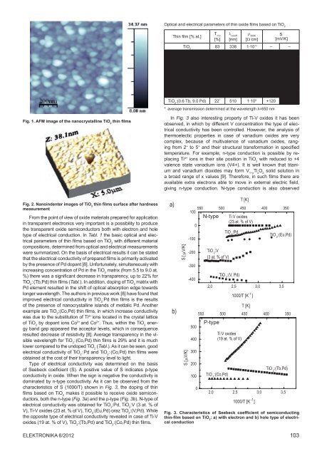
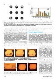
Fig. 1. AFM image <strong>of</strong> <strong>the</strong> nanocrystalline TiO 2<br />
thin films<br />
Fig. 2. Nanoindenter images <strong>of</strong> TiO 2<br />
thin films surface after hardness<br />
measurement<br />
From <strong>the</strong> point <strong>of</strong> view <strong>of</strong> oxide materials prepared for application<br />
in transparent electronics very important is a possibility to produce<br />
<strong>the</strong> transparent oxide semiconductors both with electron and hole<br />
type <strong>of</strong> electrical conduction. In Tabl. 1 <strong>the</strong> basic optical and electrical<br />
parameters <strong>of</strong> thin films based on TiO 2<br />
with different material<br />
compositions, determined from optical and electrical measurements<br />
were summarized. On <strong>the</strong> basis <strong>of</strong> electrical results it can be stated<br />
that <strong>the</strong> electrical conductivity <strong>of</strong> prepared films is primarily activated<br />
by <strong>the</strong> presence <strong>of</strong> Pd dopant [8]. Unfortunately, simultaneously with<br />
increasing concentration <strong>of</strong> Pd in <strong>the</strong> TiO 2<br />
matrix (from 5.5 to 9.0 at.<br />
%) <strong>the</strong>re was a significant decrease in transparency, up to 22% for<br />
TiO 2<br />
: (Tb,Pd) thin films (Tabl.). In addition, doping <strong>of</strong> TiO 2<br />
matrix with<br />
Pd element resulted in <strong>the</strong> shift <strong>of</strong> optical absorption edge towards<br />
longer wavelength. The authors in previous work [8] have found that<br />
improved electrical conductivity in TiO 2<br />
:Pd thin films is <strong>the</strong> results<br />
<strong>of</strong> <strong>the</strong> presence <strong>of</strong> nanocrystalline islands <strong>of</strong> mettalic Pd. Ano<strong>the</strong>r<br />
example are TiO 2<br />
:(Co,Pd) thin films, in which increase conductivity<br />
was due to <strong>the</strong> substitution <strong>of</strong> Ti 4+ ions located in <strong>the</strong> crystal lattice<br />
<strong>of</strong> TiO 2<br />
by dopant ions Co 3+ and Co 2+ . Thus, within <strong>the</strong> TiO 2<br />
energy<br />
band gap appeared <strong>the</strong> acceptor levels, which in consequence<br />
resulted decrease <strong>of</strong> resistivity [8]. Average transparency in <strong>the</strong> visible<br />
wavelength for TiO 2<br />
: (Co,Pd) thin films is 29% and it is much<br />
lower compared to <strong>the</strong> undoped TiO 2<br />
(Tabl.). As it can be seen, good<br />
electrical conductivity <strong>of</strong> TiO 2<br />
: Pd and TiO 2<br />
: (Co,Pd) thin films were<br />
obtained at <strong>the</strong> cost <strong>of</strong> <strong>the</strong>ir transparency level to light.<br />
Type <strong>of</strong> electrical conductivity was determined on <strong>the</strong> basis<br />
<strong>of</strong> Seebeck coeficient (S). A positive value <strong>of</strong> S indicates p-type<br />
conductivity in oxide. When <strong>the</strong> sign is negative <strong>the</strong> conductivity is<br />
dominated by n-type conductivity. As it can be observed from <strong>the</strong><br />
characteristics <strong>of</strong> S (1000/T) shown in Fig. 3, <strong>the</strong> doping <strong>of</strong> thin<br />
films based on TiO 2<br />
makes it possible to receive oxide semiconductors,<br />
both <strong>the</strong> n-type (Fig. 3a) and <strong>the</strong> p-type (Fig. 3b). N-type <strong>of</strong><br />
electrical conductivity was obtained for TiO 2<br />
:Pd, TiO 2<br />
:V (3 at. % <strong>of</strong><br />
V), Ti-V oxides (23 at. % <strong>of</strong> V), TiO 2<br />
:(Eu,Pd) oraz TiO 2<br />
:(V,Pd). While<br />
<strong>the</strong> opposite type <strong>of</strong> electrical conductivity revealed in case <strong>of</strong> Ti-V<br />
oxides (19 at. % <strong>of</strong> V), TiO 2<br />
:(Tb,Pd) and TiO 2<br />
:(Co,Pd) thin films.<br />
In Fig. 3 also interesting property <strong>of</strong> Ti-V oxides it has been<br />
observed, in which by different V concentration <strong>the</strong> type <strong>of</strong> electrical<br />
conductivity has been controlled. However, <strong>the</strong> analysis <strong>of</strong><br />
<strong>the</strong>rmoelectic properties in case <strong>of</strong> vanadium oxides are very<br />
complex, because <strong>of</strong> multivalence <strong>of</strong> vanadium oxides, ranging<br />
from 2 + to 5 + and <strong>the</strong>ir structural transformation in specified<br />
temperature. For example, n-type conduction is possible by replacing<br />
Ti 4+ ions in <strong>the</strong>ir site position in TiO 2<br />
with reduced to +4<br />
valence state vanadium ions (V4+). It is well known that titanium<br />
and vanadium dioxides may form V 1−x<br />
Ti x<br />
O 2<br />
solid solution in<br />
a broad range <strong>of</strong> x values [9]. Therefore, in such films <strong>the</strong>re are<br />
available extra electrons able to move in external electric field,<br />
giving n-type conduction. N-type conduction is also observed<br />
a)<br />
b)<br />
S [ µV/K]<br />
S [µV/K]<br />
550 500 450 400 350<br />
100<br />
N-type Ti:V oxides<br />
(23 at. % <strong>of</strong> V)<br />
0<br />
-100<br />
-200<br />
-300<br />
-400<br />
500<br />
400<br />
300<br />
200<br />
100<br />
0<br />
TiO 2<br />
:V<br />
(3 at. % <strong>of</strong> V)<br />
TiO 2<br />
:Pd<br />
TiO 2<br />
:(V, Pd)<br />
T [K]<br />
TiO 2<br />
:(Eu,Pd)<br />
2,0 2,5 3,0 3,5<br />
1000/T [K -1 ]<br />
550 500 450 400 350<br />
P-type<br />
Ti:V oxides<br />
(19 at. % <strong>of</strong> V)<br />
TiO 2<br />
:(Co,Pd)<br />
T [K]<br />
TiO 2<br />
:(Tb,Pd)<br />
2,0 2,5 3,0 3,5<br />
1000/T [K -1 ]<br />
Fig. 3. Characteristics <strong>of</strong> Seebeck coefficient <strong>of</strong> semiconducting<br />
thin-film based on TiO 2<br />
: a) with electron and b) hole type <strong>of</strong> electrical<br />
conduction<br />
Elektronika 6/2012 103


