

Proceedings of the European Summer School of Photovoltaics 4 â 7 ...
Proceedings of the European Summer School of Photovoltaics 4 â 7 ...
Proceedings of the European Summer School of Photovoltaics 4 â 7 ...

Create successful ePaper yourself
Turn your PDF publications into a flip-book with our unique Google optimized e-Paper software.
Photocurrent [A]<br />
a)<br />
b)<br />
104<br />
10,0p<br />
8,0p<br />
6,0p<br />
4,0p<br />
2,0p<br />
R λ<br />
[%]<br />
0,0<br />
0 500 1000 1500 2000<br />
R λ<br />
(%)<br />
100<br />
80<br />
60<br />
40<br />
20<br />
0<br />
100<br />
80<br />
60<br />
40<br />
20<br />
0<br />
X [ µm]<br />
pure, polished Si<br />
TOS-Si<br />
U=0 V<br />
λ=399 nm<br />
λ=466 nm<br />
λ=547 nm<br />
λ=589 nm<br />
λ=632 nm<br />
λ=928 nm<br />
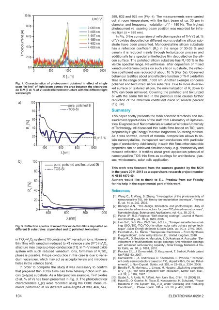
Fig. 4. Characteristics <strong>of</strong> photocurrent obtained in effect <strong>of</strong> single<br />
scan “in line” <strong>of</strong> light beam across <strong>the</strong> area between <strong>the</strong> electrodes<br />
on Ti-V (3 at. % <strong>of</strong> V) oxides/Si heterostructure with <strong>the</strong> different light<br />
wavelength<br />
400 600 800 1000<br />
λ [nm]<br />
pure, polished and texturized Si<br />
TOS-Si<br />
R λ<br />
=18 %<br />
400 600 800 1000<br />
λ (nm)<br />
Fig. 5. Reflection spectra <strong>of</strong> mixed Ti-V oxide thin films deposited on<br />
different Si substrates: a) polished and b) polished, texturized<br />
in TiO 2<br />
–V 2<br />
O 5<br />
system [10] containing V 5+ vanadium ions. However<br />
thin films with vanadium reduced to +3 valence state (V 3+ ) inV 2<br />
O 3<br />
structure may display p-type conduction [11]. In Ti–V mixed oxide<br />
system with such reduced vanadium ions, formation <strong>of</strong> V 2<br />
TiO 5<br />
phase is possible. P-type conduction in this case is due to vanadium<br />
vacancies, which may act as acceptor levels and introduce<br />
holes in <strong>the</strong> valence band.<br />
In order to complete <strong>the</strong> study it was necessary to confirm<br />
that prepared thin TOSs films can form heterojunction with silicon<br />
(p-type) substrate. As a hterojunction example, Ti-V oxides<br />
(3 at. % <strong>of</strong> V) has been presented in Fig. 3. The photoelectrical<br />
characteristics I ph<br />
(x) were recorded using <strong>the</strong> OBIC measurements<br />
performed at six different wavelengths <strong>of</strong> 399, 466, 547,<br />
589, 632 and 928 nm (Fig. 4). The measurements were carried<br />
out at room temperature, with <strong>the</strong> light beam <strong>of</strong> ca. 30 µm in<br />
diameter and frequency modulation <strong>of</strong> f = 180 Hz. The highest<br />
photocurrent vs. scaning beam position was recorded for infrared<br />
light (λ = 928 nm).<br />
In Fig. 5 <strong>the</strong> comparision <strong>of</strong> reflection spectra <strong>of</strong> Ti-V (3 at. %<br />
<strong>of</strong> V) oxides deposited on different monocrystalline silicon substrate<br />
have been presented. Monocrystalline silicon substrate<br />
has a reflection coefficient (R λ<br />
) in <strong>the</strong> range <strong>of</strong> 30-35 % and<br />
usually it is reduced mainly through texturization process and<br />
additionally by a special antireflective film deposited on <strong>the</strong> silicon<br />
surface. The polished silicon substrate has R λ<br />
=30 % in <strong>the</strong><br />
visible spectral range. Never<strong>the</strong>less, after deposition <strong>of</strong> mixed<br />
vanadium-titanium oxides on such silicon substrate, <strong>the</strong> reflection<br />
coefficient was reduced <strong>of</strong> about 10 % (Fig. 5a). Observed<br />
behaviour testifies about antireflective function <strong>of</strong> Ti-V oxide thin<br />
films in <strong>the</strong> range <strong>of</strong> 300...1000 nm. Ano<strong>the</strong>r example concerns<br />
polished and texturized silicon substrate. Due to more diversivied<br />
surface <strong>of</strong> textured silicon, <strong>the</strong> minimalization <strong>of</strong> R λ<br />
down to<br />
10% can been achieved. Covering <strong>the</strong> polished and texturized<br />
Si with <strong>the</strong> same film like in <strong>the</strong> previous case causes fur<strong>the</strong>r<br />
reduction <strong>of</strong> <strong>the</strong> reflection coefficient dwon to several percent<br />
(Fig. 5b).<br />
Summary<br />
This paper briefly presents <strong>the</strong> main scientific directions and measurement<br />
opportunities <strong>of</strong> <strong>the</strong> staff from Laboratory <strong>of</strong> Optoelectrical<br />
Diagnostics <strong>of</strong> Nanomaterials situated at Wroclaw Univeristy<br />
<strong>of</strong> Technology. All discussed thin oxide films based on TiO 2<br />
were<br />
prepared by High Energy Reactive Magnetron Sputtering method.<br />
As it was showed, control <strong>of</strong> material composition allows to obtain<br />
nanocrystalline, transparent semiconductors with particular<br />
type <strong>of</strong> conductivity. Additionally, in such thin films o<strong>the</strong>r desirable<br />
properties can be achieved simultaneously, e.g. photoactivity and<br />
reduced reflection. It testifies about great application potential <strong>of</strong><br />
nanocrystalline TOS thin films as coatings for architectural glasses,<br />
windscreens, solar cells application.<br />
This work was financed from <strong>the</strong> sources granted by <strong>the</strong> NCN<br />
in <strong>the</strong> years 2011-2013 as a supervisors research project number<br />
N N515 4970 40.<br />
Authors would like to thank to E.L. Prociow from our Faculty<br />
for his help in <strong>the</strong> experimental part <strong>of</strong> this work.<br />
References<br />
[1] Wang C., T. Wang, S. Zheng, “Investigation <strong>of</strong> <strong>the</strong> photoreactivity <strong>of</strong><br />
nanocrystalline TiO 2<br />
thin film by ion-implantation technique”, Physica<br />
E, vol. 14, p. 242, 2002.<br />
[2] Banerjee A.N., “The design, fabrication, and photocatalytic utility <strong>of</strong><br />
nanostructured semiconductors: focus on TiO 2<br />
-based nanostructures”,<br />
Nanotechnology, Science and Applications, vol. 4, p. 35, 2011.<br />
[3] Parkin I.P., R.G. Palgrave, “Self-cleaning coatings”, Journal <strong>of</strong> Materials<br />
Chemistry, vol. 15, p. 1689, 2005.<br />
[4] Lien S-Y., D-S. Wuu, W-C. Yeh, J-C. Liu, “Tri-layer antireflection coatings<br />
(SiO 2<br />
/SiO 2<br />
-TiO 2<br />
/TiO 2<br />
) for silicon solar cells using a sol-gel technique”,<br />
Solar Energy Materials & Solar Cells, vol. 90, p. 2710, 2006.<br />
[5] Facchetti A., T.J. Marks, “Transparent Electronics – From Syn<strong>the</strong>sis<br />
to Applications”, John Wiley &Sons Ltd., United Kingdom, 2010.<br />
[6] Prado R., G. Beobide, A. Marcaide, J. Goikoetxea, A. Aranzabe, “Development<br />
<strong>of</strong> multifunctional sol-gel coatings: Anti-reflection coatings<br />
with enhanced self-cleaning capacity”, Solar Energy Materials & Solar<br />
Cells, vol. 94, p. 1081, 2010.<br />
[7] Prociow E.L., J. Domaradzki, D. Kaczmarek, T. Berlicki, Polish patent<br />
No P382163, 2007.<br />
[8] Domaradzki J., A. Borkowska, D. Kaczmarek, E. Prociów, “Transparent<br />
oxide semiconductors based on TiO 2<br />
doped with V, Co and Pd elements”,<br />
J. Non-Crystall. Solids, vol. 352, nr 23–25, p. 2324, 2006.<br />
[9] Beteille F., R. Morineau, J. Livage, M. Nagano, „Switching properties<br />
<strong>of</strong> V 1−x<br />
Ti x<br />
O 2<br />
thin films deposited from alkoxides”, Mater. Res. Bull.,<br />
vol. 32, p. 1109, 1997.<br />
[10] Szabo A., A. Urda, M. Alifanti, Ann. Univ. Buc. Chim. 15 (2006) 85.<br />
[11] Habel D., O. Goerke, M. Tovar, E. Kondratenko, H. Schubert, “Phase<br />
Relations in <strong>the</strong> System TiO 2<br />
-V 2<br />
O x<br />
under Oxidizing and Reducing<br />
Conditions”, J. Phase Equilib. Diffus., vol. 29, p. 482, 2008.<br />
Elektronika 6/2012


