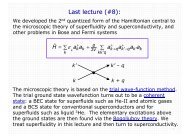
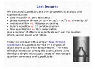
Set of supplementary notes.
Set of supplementary notes.
Set of supplementary notes.

You also want an ePaper? Increase the reach of your titles
YUMPU automatically turns print PDFs into web optimized ePapers that Google loves.
8.2. P-N JUNCTION 109<br />
p<br />
(acceptor-doped)<br />
n<br />
(donor doped)<br />
band scheme<br />
(energy levels)<br />
minority electrons<br />
conduction band<br />
valence band<br />
majority holes<br />
E j<br />
majority electrons<br />
eφ j<br />
minority holes<br />
μ<br />
Mismatch in<br />
chem. pot. μ<br />
causes charge<br />
transfer across<br />
junction, building<br />
contact potential<br />
φ j<br />
. This results<br />
in band bending,<br />
until μ equal on<br />
both sides.<br />
carrier<br />
density<br />
charge<br />
density<br />
electric<br />
field<br />
-eN a<br />
Charge transfer<br />
results in space<br />
Electrons from n-<br />
N a<br />
(acceptor density)<br />
N d<br />
(donor density) side cross<br />
the junction,<br />
annihilate holes<br />
Depletion<br />
from p-side,<br />
layer<br />
causing<br />
carrier-free zone<br />
eN d<br />
(Depletion layer)<br />
charge. Max.<br />
charge density<br />
given by dopant<br />
concentration.<br />
electrostatic<br />
potential<br />
E j<br />
junction<br />
φ j<br />
Space charge<br />
causes in-built<br />
junction field E j<br />
and contact pot.<br />
φ j<br />
, which<br />
build until chargetransfer<br />
stops.<br />
Figure 8.5: Overview <strong>of</strong> a p-n junction in equilibrium. Far away from the junction, the chemical<br />
potential µ must lie close to the bottom <strong>of</strong> the conduction band in the n-doped material, and<br />
close to the top <strong>of</strong> the valence band in the p-doped material. This is achieved by building up<br />
a contact potential φ, which shifts the energy levels as E(z) = E 0 − eφ(z). The change in<br />
potential across the junction is φ j . It gives rise to an in-built field E j .<br />
Potential barrier: The depletion regime <strong>of</strong> the junction is a high-resistance in comparison<br />
to the n- or p-type doped semiconductors. Any potential across the device is dropped almost<br />
entirely across the depletion layer. The overall potential seen by a (positively charged) hole is<br />
therefore φ j − V , where φ j is the junction potential at equilibrium.<br />
Balance <strong>of</strong> currents: In equilibrium with no external voltage bias, there is no net current<br />
flowing across the junction. We can, however, distinguish mechanisms which would drive currents<br />
across the barrier in both directions. In equilibrium, these currents cancel. We consider