Set of supplementary notes.
Set of supplementary notes.
Set of supplementary notes.

You also want an ePaper? Increase the reach of your titles
YUMPU automatically turns print PDFs into web optimized ePapers that Google loves.
8.5. COMPOUND SEMICONDUCTOR HETEROSTRUCTURES 119<br />
/(0+/-#12<br />
!<br />
,-. *<br />
*&'+<br />
+%+2')!2<br />
3!+%/<br />
!"#$%&'()<br />
inversion layer<br />
conduction band<br />
μ (semiconductor)<br />
E c<br />
-eφ(z)<br />
E v<br />
-eφ(z)<br />
#<br />
"<br />
μ (metal)<br />
eV<br />
valence band<br />
(chemical potentials<br />
do not have to line<br />
up, because insulator<br />
blocks current flow.)<br />
"<br />
Metal<br />
Insulator<br />
p-type semiconductor<br />
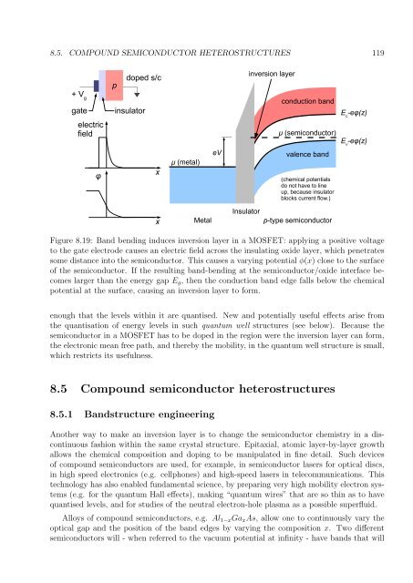
Figure 8.19: Band bending induces inversion layer in a MOSFET: applying a positive voltage<br />
to the gate electrode causes an electric field across the insulating oxide layer, which penetrates<br />
some distance into the semiconductor. This causes a varying potential φ(x) close to the surface<br />
<strong>of</strong> the semiconductor. If the resulting band-bending at the semiconductor/oxide interface becomes<br />
larger than the energy gap E g , then the conduction band edge falls below the chemical<br />
potential at the surface, causing an inversion layer to form.<br />
enough that the levels within it are quantised. New and potentially useful effects arise from<br />
the quantisation <strong>of</strong> energy levels in such quantum well structures (see below). Because the<br />
semiconductor in a MOSFET has to be doped in the region were the inversion layer can form,<br />
the electronic mean free path, and thereby the mobility, in the quantum well structure is small,<br />
which restricts its usefulness.<br />
8.5 Compound semiconductor heterostructures<br />
8.5.1 Bandstructure engineering<br />
Another way to make an inversion layer is to change the semiconductor chemistry in a discontinuous<br />
fashion within the same crystal structure. Epitaxial, atomic layer-by-layer growth<br />
allows the chemical composition and doping to be manipulated in fine detail. Such devices<br />
<strong>of</strong> compound semiconductors are used, for example, in semiconductor lasers for optical discs,<br />
in high speed electronics (e.g. cellphones) and high-speed lasers in telecommunications. This<br />
technology has also enabled fundamental science, by preparing very high mobility electron systems<br />
(e.g. for the quantum Hall effects), making “quantum wires” that are so thin as to have<br />
quantised levels, and for studies <strong>of</strong> the neutral electron-hole plasma as a possible superfluid.<br />
Alloys <strong>of</strong> compound semiconductors, e.g. Al 1−x Ga x As, allow one to continuously vary the<br />
optical gap and the position <strong>of</strong> the band edges by varying the composition x. Two different<br />
semiconductors will - when referred to the vacuum potential at infinity - have bands that will