Service Manual - AMS Neve
Service Manual - AMS Neve
Service Manual - AMS Neve

Create successful ePaper yourself
Turn your PDF publications into a flip-book with our unique Google optimized e-Paper software.
CIRCUIT DESCRIPTION<br />
SynchroNet ES/2 <strong>Service</strong> <strong>Manual</strong><br />
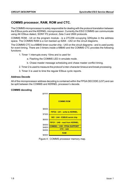
COMMS processor, RAM, ROM and CTC.<br />
The COMMS microprocessor is solely responsible for dealing with the protocol translation between<br />
the ESbus ports and the KERNEL microprocessor. Currently the ES/2 COMMS can communicate<br />
using AK ESbus dialect, SONY P2 protocol, Zeta 3 and 2600 protocols.<br />
COMMS ROM - U4 on the program module - is a 27C256 occupying 32Kbytes in the address<br />
space. The COMMS RAM is a non backed up 6264 - U42 on the circuit diagrams.<br />
The COMMS CTC is a 68B40 timer counter chip - U43 on the circuit diagrams - and is used purely<br />
for event timing. There are 3 timers inside a 68B40 and the COMMS CTC provides the following<br />
functions:<br />
1. Timer 1 interrupts every 10ms and is used for:<br />
a. Flashing the COMMS LED in emulate mode.<br />
b. Chase master message scheduling and chase master conflict timing.<br />
2. Timer 2 is used to measure the protocol’s inter-character timeout and break processing.<br />
3. Timer 3 is used to time the regular ESbus cyclic reports.<br />
Address Decode<br />
All of the microprocessor address decoding is contained within the FPGA DECODE (U37) and can<br />
be split between the COMMS and KERNEL processor’s decode.<br />
COMMS decoding<br />
$FFFF -<br />
COMMS ROM<br />
$8000 -<br />
$7000 -<br />
FIFO2 : U41 - write to KERNEL<br />
SIO : U44 - ESBUS serial chip<br />
$6000 -<br />
FIFO1 : U40 - read from KERNEL<br />
$5000 -<br />
COMSEL : U39 - FPGA SUPPORT<br />
$4800 -<br />
CTC : U43<br />
$4000 -<br />
RAM<br />
$0000 -<br />
Figure 4 : COMMS processor memory map.<br />
1:8 Issue 1