Service Manual - AMS Neve
Service Manual - AMS Neve
Service Manual - AMS Neve

You also want an ePaper? Increase the reach of your titles
YUMPU automatically turns print PDFs into web optimized ePapers that Google loves.
SynchroNet ES/2 <strong>Service</strong> <strong>Manual</strong><br />
CIRCUIT DESCRIPTION<br />
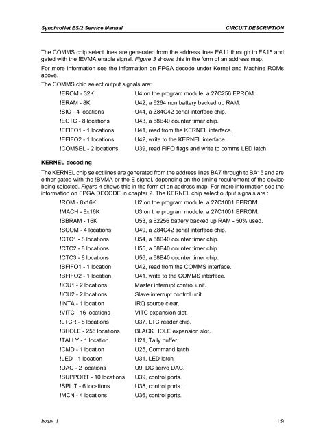
The COMMS chip select lines are generated from the address lines EA11 through to EA15 and<br />
gated with the !EVMA enable signal. Figure 3 shows this in the form of an address map.<br />
For more information see the information on FPGA decode under Kernel and Machine ROMs<br />
above.<br />
The COMMS chip select output signals are:<br />
!EROM - 32K<br />
U4 on the program module, a 27C256 EPROM.<br />
!ERAM - 8K<br />
U42, a 6264 non battery backed up RAM.<br />
!SIO - 4 locations<br />
U44, a Z84C42 serial interface chip.<br />
!ECTC - 8 locations U43, a 68B40 counter timer chip.<br />
!EFIFO1 - 1 locations U41, read from the KERNEL interface.<br />
!EFIFO2 - 1 locations U42, write to the KERNEL interface.<br />
!COMSEL - 2 locations U39, read FIFO flags and write to comms LED latch<br />
KERNEL decoding<br />
The KERNEL chip select lines are generated from the address lines BA7 through to BA15 and are<br />
either gated with the !BVMA or the E signal, depending on the timing requirement of the device<br />
being selected. Figure 4 shows this in the form of an address map. For more information see the<br />
information on FPGA DECODE in chapter 2. The KERNEL chip select output signals are :<br />
!ROM - 8x16K<br />
U2 on the program module, a 27C1001 EPROM.<br />
!MACH - 8x16K<br />
U3 on the program module, a 27C1001 EPROM.<br />
!BBRAM - 16K<br />
U53, a 62256 battery backed up RAM - 50% used.<br />
!SCOM - 4 locations U49, a Z84C42 serial interface chip.<br />
!CTC1 - 8 locations U54, a 68B40 counter timer chip.<br />
!CTC2 - 8 locations U55, a 68B40 counter timer chip.<br />
!CTC3 - 8 locations U56, a 68B40 counter timer chip.<br />
!BFIFO1 - 1 location U42, read from the COMMS interface.<br />
!BFIFO2 - 1 location U41, write to the COMMS interface.<br />
!ICU1 - 2 locations Master interrupt control unit.<br />
!ICU2 - 2 locations Slave interrupt control unit.<br />
!INTA - 1 location<br />
IRQ source clear.<br />
!VITC - 16 locations VITC expansion slot.<br />
!LTCR - 8 locations U37, LTC reader chip.<br />
!BHOLE - 256 locations BLACK HOLE expansion slot.<br />
!TALLY - 1 location U21, Tally buffer.<br />
!CMD - 1 location<br />
U25, Command latch<br />
!LED - 1 location<br />
U31, LED latch<br />
!DAC - 2 locations<br />
U9, DC servo DAC.<br />
!SUPPORT - 10 locations U39, control ports.<br />
!SPLIT - 6 locations U38, control ports.<br />
!MCN - 4 locations U36, control ports.<br />
Issue 1 1:9