

Design and Realization of a Prototype Hardware Platform for ...
Design and Realization of a Prototype Hardware Platform for ...
Design and Realization of a Prototype Hardware Platform for ...

You also want an ePaper? Increase the reach of your titles
YUMPU automatically turns print PDFs into web optimized ePapers that Google loves.
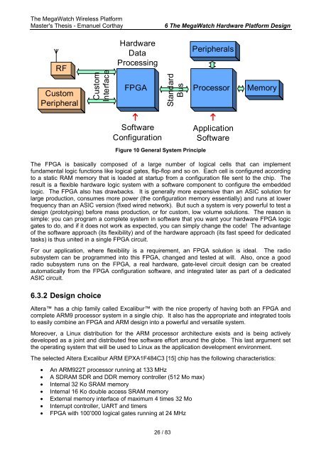
The MegaWatch Wireless <strong>Plat<strong>for</strong>m</strong>Master's Thesis - Emanuel Corthay6 The MegaWatch <strong>Hardware</strong> <strong>Plat<strong>for</strong>m</strong> <strong>Design</strong>RFCustomPeripheralCustomInterface<strong>Hardware</strong>DataProcessingFPGASt<strong>and</strong>ardBusPeripheralsProcessorMemoryS<strong>of</strong>twareConfigurationFigure 10 General System PrincipleApplicationS<strong>of</strong>twareThe FPGA is basically composed <strong>of</strong> a large number <strong>of</strong> logical cells that can implementfundamental logic functions like logical gates, flip-flop <strong>and</strong> so on. Each cell is configured accordingto a static RAM memory that is loaded at startup from a configuration file sent to the chip. Theresult is a flexible hardware logic system with a s<strong>of</strong>tware component to configure the embeddedlogic. The FPGA also has drawbacks. It is generally more expensive than an ASIC solution <strong>for</strong>large production, consumes more power (the configuration memory essentially) <strong>and</strong> runs at lowerfrequency than an ASIC version (fixed wired network). But such a system is very powerful to test adesign (prototyping) be<strong>for</strong>e mass production, or <strong>for</strong> custom, low volume solutions. The reason issimple: you can program a complete system in s<strong>of</strong>tware that you want your hardware FPGA logicgates to do, <strong>and</strong> if it does not work as expected, you can simply change the code! The advantage<strong>of</strong> the s<strong>of</strong>tware approach (its flexibility) <strong>and</strong> <strong>of</strong> the hardware approach (its fast speed <strong>for</strong> dedicatedtasks) is thus united in a single FPGA circuit.For our application, where flexibility is a requirement, an FPGA solution is ideal. The radiosubsystem can be programmed into this FPGA, changed <strong>and</strong> tested at will. Also, once a goodradio subsystem runs on the FPGA, a real hardware, gate-level circuit design can be createdautomatically from the FPGA configuration s<strong>of</strong>tware, <strong>and</strong> integrated later as part <strong>of</strong> a dedicatedASIC circuit.6.3.2 <strong>Design</strong> choiceAltera has a chip family called Excalibur with the nice property <strong>of</strong> having both an FPGA <strong>and</strong>complete ARM9 processor system in a single chip. It also has the appropriate <strong>and</strong> integrated toolsto easily combine an FPGA <strong>and</strong> ARM design into a powerful <strong>and</strong> versatile system.Moreover, a Linux distribution <strong>for</strong> the ARM processor architecture exists <strong>and</strong> is being activelydeveloped as a joint <strong>and</strong> distributed free s<strong>of</strong>tware ef<strong>for</strong>t around the globe. This last argument setthe operating system that will be used to Linux as the application development environment.The selected Altera Excalibur ARM EPXA1F484C3 [15] chip has the following characteristics:• An ARM922T processor running at 133 MHz• A SDRAM SDR <strong>and</strong> DDR memory controller (512 Mo max)• Internal 32 Ko SRAM memory• Internal 16 Ko double access SRAM memory• External memory interface <strong>of</strong> maximum 4 times 32 Mo• Interrupt controller, UART <strong>and</strong> timers• FPGA with 100’000 logical gates running at 24 MHz26 / 83


