

Design and Realization of a Prototype Hardware Platform for ...
Design and Realization of a Prototype Hardware Platform for ...
Design and Realization of a Prototype Hardware Platform for ...

Create successful ePaper yourself
Turn your PDF publications into a flip-book with our unique Google optimized e-Paper software.
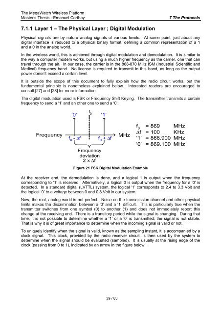
The MegaWatch Wireless <strong>Plat<strong>for</strong>m</strong>Master's Thesis - Emanuel Corthay7 The Protocols7.1.1 Layer 1 – The Physical Layer ; Digital ModulationPhysical signals are by nature analog signals <strong>of</strong> various levels. At some point, just about anydigital interface is reduced to a physical binary <strong>for</strong>mat, defining a common representation <strong>of</strong> a 1<strong>and</strong> a 0 in the analog world.In the wireless world, this is achieved through digital modulation <strong>and</strong> demodulation. It is similar tothe way a computer modem works, but using a much higher frequency as the carrier, one that cantravel through the air. In our case, the carrier is in the 868-870 MHz ISM (Industrial Scientific <strong>and</strong>Medical) frequency b<strong>and</strong>. No license is required to transmit in this b<strong>and</strong>, as long as the outputpower doesn’t exceed a certain level.It is outside the scope <strong>of</strong> this document to fully explain how the radio circuit works, but thefundamental principle is nonetheless explained below. Interested readers are encouraged toconsult [27] <strong>and</strong> [28] <strong>for</strong> more in<strong>for</strong>mation.The digital modulation used is FSK or Frequency Shift Keying. The transmitter transmits a certainfrequency to send a ‘1’ <strong>and</strong> an other one to send a ‘0’:‘0’f 0‘1’Frequencyf 0- ∆fFrequencydeviation2 x ∆ff 0+ ∆fMHzFigure 21 FSK Digital Modulation Examplef 0= 869 MHz∆f = 100 KHz‘1’ = 868.900 MHz‘0’ = 869.100 MHzAt the receiver end, the demodulation is done, <strong>and</strong> a logical 1 is output when the frequencycorresponding to ‘1’ is received. Alternatively, a logical 0 is output when the frequency <strong>for</strong> a ‘0’ isdetected. In a st<strong>and</strong>ard digital (LVTTL) system, the logical ‘1’ corresponds to 2.4 to 3.3 Volt <strong>and</strong>the logical ‘0’ to a voltage between 0 <strong>and</strong> 0.8 Volt in our system.Now, the real, analog world is not perfect. Noise on the transmission channel <strong>and</strong> other physicallimits makes the discrimination between a ‘0’ <strong>and</strong> a ‘1’ difficult. This is particularly true when thetransmitter switches from one symbol (0) to another (1) <strong>and</strong> does not immediately report thischange at the receiving end. There is a transitory period while the signal is changing. During thattime, it is not possible to determine whether a ‘1’ or a ‘0’ is transmitted; the signal is not stable.That is why it is <strong>of</strong> great importance to determine when the incoming signal is valid or not.To uniquely identify when the signal is valid, known as the sampling instant, it is accompanied by aclock signal. This clock, provided by the radio receiver circuit, is then used by the system todetermine when the signal should be evaluated (sampled). It is usually at the rising edge <strong>of</strong> theclock (passing from 0 to 1), indicated by an arrow in the figure below.39 / 83


