

Design and Realization of a Prototype Hardware Platform for ...
Design and Realization of a Prototype Hardware Platform for ...
Design and Realization of a Prototype Hardware Platform for ...

You also want an ePaper? Increase the reach of your titles
YUMPU automatically turns print PDFs into web optimized ePapers that Google loves.
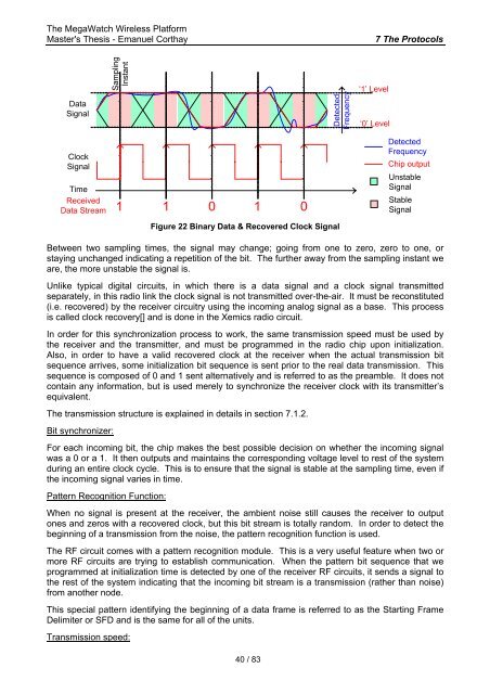
The MegaWatch Wireless <strong>Plat<strong>for</strong>m</strong>Master's Thesis - Emanuel Corthay7 The ProtocolsDataSignalClockSignalTimeReceivedData StreamSamplingInstant1 1 0 1 0DetectedFrequency‘1’ Level‘0’ LevelDetectedFrequencyChip outputUnstableSignalStableSignalFigure 22 Binary Data & Recovered Clock SignalBetween two sampling times, the signal may change; going from one to zero, zero to one, orstaying unchanged indicating a repetition <strong>of</strong> the bit. The further away from the sampling instant weare, the more unstable the signal is.Unlike typical digital circuits, in which there is a data signal <strong>and</strong> a clock signal transmittedseparately, in this radio link the clock signal is not transmitted over-the-air. It must be reconstituted(i.e. recovered) by the receiver circuitry using the incoming analog signal as a base. This processis called clock recovery[] <strong>and</strong> is done in the Xemics radio circuit.In order <strong>for</strong> this synchronization process to work, the same transmission speed must be used bythe receiver <strong>and</strong> the transmitter, <strong>and</strong> must be programmed in the radio chip upon initialization.Also, in order to have a valid recovered clock at the receiver when the actual transmission bitsequence arrives, some initialization bit sequence is sent prior to the real data transmission. Thissequence is composed <strong>of</strong> 0 <strong>and</strong> 1 sent alternatively <strong>and</strong> is referred to as the preamble. It does notcontain any in<strong>for</strong>mation, but is used merely to synchronize the receiver clock with its transmitter’sequivalent.The transmission structure is explained in details in section 7.1.2.Bit synchronizer:For each incoming bit, the chip makes the best possible decision on whether the incoming signalwas a 0 or a 1. It then outputs <strong>and</strong> maintains the corresponding voltage level to rest <strong>of</strong> the systemduring an entire clock cycle. This is to ensure that the signal is stable at the sampling time, even ifthe incoming signal varies in time.Pattern Recognition Function:When no signal is present at the receiver, the ambient noise still causes the receiver to outputones <strong>and</strong> zeros with a recovered clock, but this bit stream is totally r<strong>and</strong>om. In order to detect thebeginning <strong>of</strong> a transmission from the noise, the pattern recognition function is used.The RF circuit comes with a pattern recognition module. This is a very useful feature when two ormore RF circuits are trying to establish communication. When the pattern bit sequence that weprogrammed at initialization time is detected by one <strong>of</strong> the receiver RF circuits, it sends a signal tothe rest <strong>of</strong> the system indicating that the incoming bit stream is a transmission (rather than noise)from another node.This special pattern identifying the beginning <strong>of</strong> a data frame is referred to as the Starting FrameDelimiter or SFD <strong>and</strong> is the same <strong>for</strong> all <strong>of</strong> the units.Transmission speed:40 / 83


