

Design and Realization of a Prototype Hardware Platform for ...
Design and Realization of a Prototype Hardware Platform for ...
Design and Realization of a Prototype Hardware Platform for ...

Create successful ePaper yourself
Turn your PDF publications into a flip-book with our unique Google optimized e-Paper software.
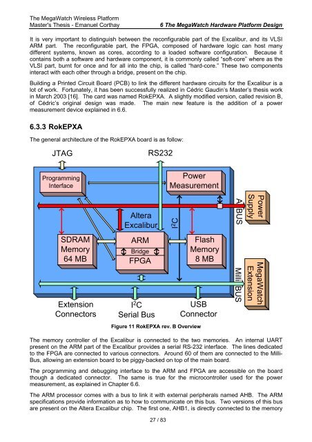
The MegaWatch Wireless <strong>Plat<strong>for</strong>m</strong>Master's Thesis - Emanuel Corthay6 The MegaWatch <strong>Hardware</strong> <strong>Plat<strong>for</strong>m</strong> <strong>Design</strong>It is very important to distinguish between the reconfigurable part <strong>of</strong> the Excalibur, <strong>and</strong> its VLSIARM part. The reconfigurable part, the FPGA, composed <strong>of</strong> hardware logic can host manydifferent systems, known as cores, according to a loaded s<strong>of</strong>tware configuration. Because itcontains both a s<strong>of</strong>tware <strong>and</strong> hardware component, it is commonly called “s<strong>of</strong>t-core” where as theVLSI part, burnt <strong>for</strong> once <strong>and</strong> <strong>for</strong> all into the chip, is called “hard-core.” These two componentsinteract with each other through a bridge, present on the chip.Building a Printed Circuit Board (PCB) to link the different hardware circuits <strong>for</strong> the Excalibur is alot <strong>of</strong> work. Fortunately, it has been successfully realized in Cédric Gaudin’s Master’s thesis workin March 2003 [16]. The card was named RokEPXA. A slightly modified version, called revision B,<strong>of</strong> Cédric’s original design was made. The main new feature is the addition <strong>of</strong> a powermeasurement device explained in 6.6.6.3.3 RokEPXAThe general architecture <strong>of</strong> the RokEPXA board is as follow:JTAGProgrammingInterfaceRS232PowerMeasurementAlteraExcaliburI 2 CA BUSPowerSupplySDRAMMemory64 MBExtensionConnectorsARMBridgeFPGAI 2 CSerial BusFlashMemory8 MBUSBConnectorFigure 11 RokEPXA rev. B OverviewMilli BUSMegaWatchExtensionThe memory controller <strong>of</strong> the Excalibur is connected to the two memories. An internal UARTpresent on the ARM part <strong>of</strong> the Excalibur provides a serial RS-232 interface. The lines dedicatedto the FPGA are connected to various connectors. Around 60 <strong>of</strong> them are connected to the Milli-Bus, allowing an extension board to be piggy-backed on top <strong>of</strong> the main board.The programming <strong>and</strong> debugging interface to the ARM <strong>and</strong> FPGA are accessible on the boardthough a dedicated connector. The same is true <strong>for</strong> the microcontroller used <strong>for</strong> the powermeasurement, as explained in Chapter 6.6.The ARM processor comes with a bus to link it with external peripherals named AHB. The ARMspecifications provide in<strong>for</strong>mation as to how to communicate on this bus. Two versions <strong>of</strong> this busare present on the Altera Excalibur chip. The first one, AHB1, is directly connected to the memory27 / 83


