- Page 2 and 3:
Direct Energy Conversion by Andrea
- Page 4 and 5:
CONTENTS i Contents Contents i 1 In
- Page 6 and 7:
CONTENTS iii 6.3.2 Energy Levels in
- Page 8 and 9:
CONTENTS v 9.6 Fuel Cells . . . . .
- Page 10:
Acknowledgements I would like to th
- Page 13 and 14:
2 1.2 Preview of Topics to connect
- Page 15 and 16:
4 1.2 Preview of Topics Math throug
- Page 17 and 18:
6 1.2 Preview of Topics Process Spo
- Page 19 and 20:
8 1.2 Preview of Topics drodynamic
- Page 21 and 22:
10 1.4 Measures of Power and Energy
- Page 23 and 24:
12 1.5 Properties of Materials 1.5
- Page 25 and 26:
14 1.5 Properties of Materials most
- Page 27 and 28:
16 1.6 Electromagnetic Waves −→
- Page 29 and 30:
18 1.6 Electromagnetic Waves Relate
- Page 31 and 32:
20 1.6 Electromagnetic Waves A unif
- Page 33 and 34:
22 1.7 Problems
- Page 35 and 36:
24 2.2 Capacitors 2.2 Capacitors 2.
- Page 37 and 38:
26 2.2 Capacitors 2.2.3 Permittivit
- Page 39 and 40:
28 2.2 Capacitors â z â y â x No
- Page 41 and 42:
30 2.2 Capacitors Figure 2.3: Natur
- Page 43 and 44:
32 2.3 Piezoelectric Devices Piezoe
- Page 45 and 46:
34 2.3 Piezoelectric Devices Lattic
- Page 47 and 48:
36 2.3 Piezoelectric Devices Herman
- Page 49 and 50:
38 2.3 Piezoelectric Devices Figure
- Page 51 and 52:
40 2.3 Piezoelectric Devices c a β
- Page 53 and 54:
42 2.3 Piezoelectric Devices In cer
- Page 55 and 56:
44 2.3 Piezoelectric Devices made m
- Page 57 and 58:
46 2.3 Piezoelectric Devices tions.
- Page 59 and 60:
48 2.4 Problems 2.5. A piezoelectri
- Page 61 and 62:
50 2.4 Problems 2.13. Consider a pi
- Page 63 and 64:
52 2.4 Problems 2.16. The gure belo
- Page 65 and 66:
54 3.2 Pyroelectricity Material Che
- Page 67 and 68:
56 3.3 Electro-Optics KH 2 PO 4 [25
- Page 69 and 70:
58 3.3 Electro-Optics The rst two t
- Page 71 and 72:
60 3.3 Electro-Optics used as an el
- Page 73 and 74:
62 3.4 Notation Quagmire Notation i
- Page 75 and 76:
64 3.5 Problems 3.5 Problems 3.1. F
- Page 77 and 78:
66 3.5 Problems −→ DinC/m 2 unp
- Page 79 and 80:
68 4.1 Introduction Center-fed half
- Page 81 and 82:
70 4.2 Electromagnetic Radiation In
- Page 83 and 84:
72 4.2 Electromagnetic Radiation ar
- Page 85 and 86:
74 4.3 Antenna Components and Denit
- Page 87 and 88:
76 4.4 Antenna Characteristics ante
- Page 89 and 90:
78 4.4 Antenna Characteristics Impe
- Page 91 and 92:
80 4.4 Antenna Characteristics Azim
- Page 93 and 94:
82 4.4 Antenna Characteristics 4.4.
- Page 95 and 96: 84 4.4 Antenna Characteristics 5 Li
- Page 97 and 98: 86 4.5 Problems Figure 4.6: A snow
- Page 99 and 100: 88 4.5 Problems 4.5. Match the foll
- Page 101 and 102: 90 4.5 Problems 4.8. Radiation patt
- Page 103 and 104: 92 5.2 Physics of the Hall Eect The
- Page 105 and 106: 94 5.2 Physics of the Hall Eect The
- Page 107 and 108: 96 5.3 Magnetohydrodynamics This am
- Page 109 and 110: 98 5.5 Applications of Hall Eect De
- Page 111 and 112: 100 5.6 Problems 5.6 Problems 5.1.
- Page 113 and 114: 102 6.2 The Wave and Particle Natur
- Page 115 and 116: 104 6.3 Semiconductors and Energy L
- Page 117 and 118: 106 6.3 Semiconductors and Energy L
- Page 119 and 120: 108 6.3 Semiconductors and Energy L
- Page 121 and 122: 110 6.3 Semiconductors and Energy L
- Page 123 and 124: 112 6.3 Semiconductors and Energy L
- Page 125 and 126: 114 6.3 Semiconductors and Energy L
- Page 127 and 128: 116 6.3 Semiconductors and Energy L
- Page 129 and 130: 118 6.3 Semiconductors and Energy L
- Page 131 and 132: 120 6.4 Crystallography Revisited L
- Page 133 and 134: 122 6.5 Pn Junctions E Indirect Sem
- Page 135 and 136: 124 6.5 Pn Junctions an excess of n
- Page 137 and 138: 126 6.5 Pn Junctions V x - + Energy
- Page 139 and 140: 128 6.6 Solar Cells to day and loca
- Page 141 and 142: 130 6.6 Solar Cells dot based mater
- Page 143 and 144: 132 6.7 Photodetectors Solar Panel
- Page 145: 134 6.7 Photodetectors 6.7.2 Measur
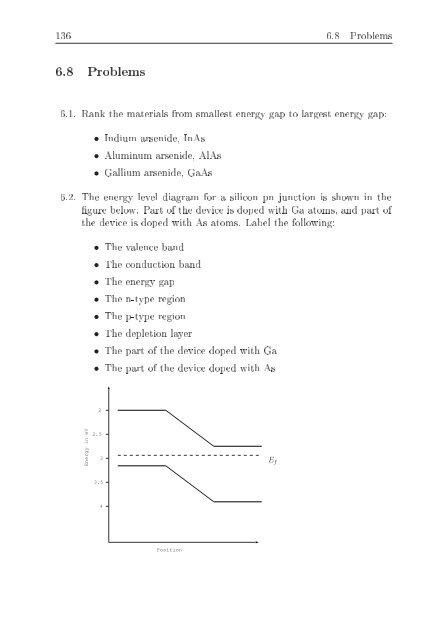
- Page 149 and 150: 138 6.8 Problems 6.6. Use Fig. 6.6
- Page 151 and 152: 140 7.2 Absorption, Spontaneous Emi
- Page 153 and 154: 400
- Page 155 and 156: 144 7.2 Absorption, Spontaneous Emi
- Page 157 and 158: 146 7.2 Absorption, Spontaneous Emi
- Page 159 and 160: 148 7.3 Devices Involving Spontaneo
- Page 161 and 162: 150 7.3 Devices Involving Spontaneo
- Page 163 and 164: 152 7.4 Devices Involving Stimulate
- Page 165 and 166: 154 7.4 Devices Involving Stimulate
- Page 167 and 168: 156 7.4 Devices Involving Stimulate
- Page 169 and 170: 158 7.4 Devices Involving Stimulate
- Page 171 and 172: 160 7.4 Devices Involving Stimulate
- Page 173 and 174: 162 7.4 Devices Involving Stimulate
- Page 175 and 176: 164 7.4 Devices Involving Stimulate
- Page 177 and 178: 166 7.5 Relationship Between Device
- Page 179 and 180: 168 7.5 Relationship Between Device
- Page 181 and 182: 170 7.6 Problems (c) Find the value
- Page 183 and 184: 172 7.6 Problems 7.10. Three main c
- Page 185 and 186: 174 8.2 Thermodynamic Properties Un
- Page 187 and 188: 176 8.3 Bulk Modulus and Related Me
- Page 189 and 190: 178 8.4 Ideal Gas Law 8.4 Ideal Gas
- Page 191 and 192: 180 8.6 Thermoelectric Eects heater
- Page 193 and 194: 182 8.6 Thermoelectric Eects charge
- Page 195 and 196: 184 8.6 Thermoelectric Eects In thi
- Page 197 and 198:
186 8.6 Thermoelectric Eects conduc
- Page 199 and 200:
188 8.7 Thermoelectric Eciency comp
- Page 201 and 202:
190 8.7 Thermoelectric Eciency Eq.
- Page 203 and 204:
192 8.8 Applications of Thermoelect
- Page 205 and 206:
194 8.8 Applications of Thermoelect
- Page 207 and 208:
196 8.9 Problems 8.6. Match the des
- Page 209 and 210:
198 8.9 Problems • Thermoelectric
- Page 212 and 213:
9 BATTERIES AND FUEL CELLS 201 9 Ba
- Page 214 and 215:
9 BATTERIES AND FUEL CELLS 203 0 En
- Page 216 and 217:
9 BATTERIES AND FUEL CELLS 205 9.1,
- Page 218 and 219:
9 BATTERIES AND FUEL CELLS 207 Both
- Page 220 and 221:
9 BATTERIES AND FUEL CELLS 209 The
- Page 222 and 223:
9 BATTERIES AND FUEL CELLS 211 9.3
- Page 224 and 225:
9 BATTERIES AND FUEL CELLS 213 e
- Page 226 and 227:
9 BATTERIES AND FUEL CELLS 215 e
- Page 228 and 229:
9 BATTERIES AND FUEL CELLS 217 E 0
- Page 230 and 231:
9 BATTERIES AND FUEL CELLS 219 The
- Page 232 and 233:
9 BATTERIES AND FUEL CELLS 221 quot
- Page 234 and 235:
9 BATTERIES AND FUEL CELLS 223 devi
- Page 236 and 237:
9 BATTERIES AND FUEL CELLS 225 Exam
- Page 238 and 239:
9 BATTERIES AND FUEL CELLS 227 Figu
- Page 240 and 241:
9 BATTERIES AND FUEL CELLS 229 were
- Page 242 and 243:
9 BATTERIES AND FUEL CELLS 231 syst
- Page 244 and 245:
9 BATTERIES AND FUEL CELLS 233 Figu
- Page 246 and 247:
9 BATTERIES AND FUEL CELLS 235 9.5.
- Page 248 and 249:
10 MISCELLANEOUS ENERGY CONVERSION
- Page 250 and 251:
10 MISCELLANEOUS ENERGY CONVERSION
- Page 252 and 253:
10 MISCELLANEOUS ENERGY CONVERSION
- Page 254 and 255:
10 MISCELLANEOUS ENERGY CONVERSION
- Page 256 and 257:
11 CALCULUS OF VARIATIONS 245 Part
- Page 258 and 259:
11 CALCULUS OF VARIATIONS 247 Many
- Page 260 and 261:
11 CALCULUS OF VARIATIONS 249 11.4
- Page 262 and 263:
11 CALCULUS OF VARIATIONS 251 We ha
- Page 264 and 265:
11 CALCULUS OF VARIATIONS 253 The L
- Page 266 and 267:
11 CALCULUS OF VARIATIONS 255 The p
- Page 268 and 269:
11 CALCULUS OF VARIATIONS 257 Energ
- Page 270 and 271:
11 CALCULUS OF VARIATIONS 259 The e
- Page 272 and 273:
11 CALCULUS OF VARIATIONS 261 Energ
- Page 274 and 275:
11 CALCULUS OF VARIATIONS 263 The a
- Page 276 and 277:
11 CALCULUS OF VARIATIONS 265 The d
- Page 278 and 279:
11 CALCULUS OF VARIATIONS 267 11.8.
- Page 280 and 281:
12 RELATING ENERGY CONVERSION PROCE
- Page 282 and 283:
12 RELATING ENERGY CONVERSION PROCE
- Page 284 and 285:
12 RELATING ENERGY CONVERSION PROCE
- Page 286 and 287:
12 RELATING ENERGY CONVERSION PROCE
- Page 288 and 289:
12 RELATING ENERGY CONVERSION PROCE
- Page 290 and 291:
12 RELATING ENERGY CONVERSION PROCE
- Page 292 and 293:
12 RELATING ENERGY CONVERSION PROCE
- Page 294 and 295:
12 RELATING ENERGY CONVERSION PROCE
- Page 296 and 297:
12 RELATING ENERGY CONVERSION PROCE
- Page 298 and 299:
12 RELATING ENERGY CONVERSION PROCE
- Page 300 and 301:
12 RELATING ENERGY CONVERSION PROCE
- Page 302 and 303:
13 THOMAS FERMI ANALYSIS 291 13 Tho
- Page 304 and 305:
13 THOMAS FERMI ANALYSIS 293 13.2 P
- Page 306 and 307:
13 THOMAS FERMI ANALYSIS 295 Symbol
- Page 308 and 309:
13 THOMAS FERMI ANALYSIS 297 Electr
- Page 310 and 311:
13 THOMAS FERMI ANALYSIS 299 Rememb
- Page 312 and 313:
13 THOMAS FERMI ANALYSIS 301 the wa
- Page 314 and 315:
13 THOMAS FERMI ANALYSIS 303 We kno
- Page 316 and 317:
13 THOMAS FERMI ANALYSIS 305 E f =
- Page 318 and 319:
13 THOMAS FERMI ANALYSIS 307 Eq. 13
- Page 320 and 321:
13 THOMAS FERMI ANALYSIS 309 functi
- Page 322 and 323:
14 LIE ANALYSIS 311 14 Lie Analysis
- Page 324 and 325:
14 LIE ANALYSIS 313 independent var
- Page 326 and 327:
14 LIE ANALYSIS 315 14.3 Continuous
- Page 328 and 329:
14 LIE ANALYSIS 317 Figure 14.1: Th
- Page 330 and 331:
14 LIE ANALYSIS 319 and y → y(1 +
- Page 332 and 333:
14 LIE ANALYSIS 321 Group property
- Page 334 and 335:
14 LIE ANALYSIS 323 pr (n) UF =0. (
- Page 336 and 337:
14 LIE ANALYSIS 325 Eqs. 14.54, 14.
- Page 338 and 339:
14 LIE ANALYSIS 327 equation must a
- Page 340 and 341:
14 LIE ANALYSIS 329 The rst term is
- Page 342 and 343:
14 LIE ANALYSIS 331 to nd the corre
- Page 344 and 345:
14 LIE ANALYSIS 333 dG [ ] dt = ξ
- Page 346 and 347:
14 LIE ANALYSIS 335 Use Eq. 14.117
- Page 348 and 349:
14 LIE ANALYSIS 337 14.7 Problems 1
- Page 350 and 351:
14 LIE ANALYSIS 339 14.9. In Proble
- Page 352 and 353:
Appendices 341 Appendices Appendix
- Page 354 and 355:
Appendices 343 Symbol Quantity Unit
- Page 356 and 357:
Appendices 345 Symbol Quantity Unit
- Page 358 and 359:
Appendices 347 Symbol Quantity Unit
- Page 360 and 361:
Appendices 349 Appendix B: Abbrevia
- Page 362 and 363:
Appendices 351 Appendix C: Overload
- Page 364 and 365:
Appendices 353 κ describes the abi
- Page 366 and 367:
REFERENCES 355 References [1] W. H.
- Page 368 and 369:
REFERENCES 357 [30] Crystal systems
- Page 370 and 371:
REFERENCES 359 [61] B. D. Iverson a
- Page 372 and 373:
REFERENCES 361 [88] M. F. Gendre, T
- Page 374 and 375:
REFERENCES 363 [115] R. Venkatasubr
- Page 376 and 377:
REFERENCES 365 [137] S. G. Bratsch,
- Page 378 and 379:
REFERENCES 367 [163] B. V. Brunt, T
- Page 380 and 381:
REFERENCES 369 [189] L. V. Ovsianni
- Page 382 and 383:
INDEX 371 Energy conservation, 9 En
- Page 384 and 385:
INDEX 373 Thomas Fermi analysis, 29