
You also want an ePaper? Increase the reach of your titles
YUMPU automatically turns print PDFs into web optimized ePapers that Google loves.
Numonyx <strong>Wireless</strong> <strong>Flash</strong> <strong>Memory</strong> (<strong>W30</strong>)<br />
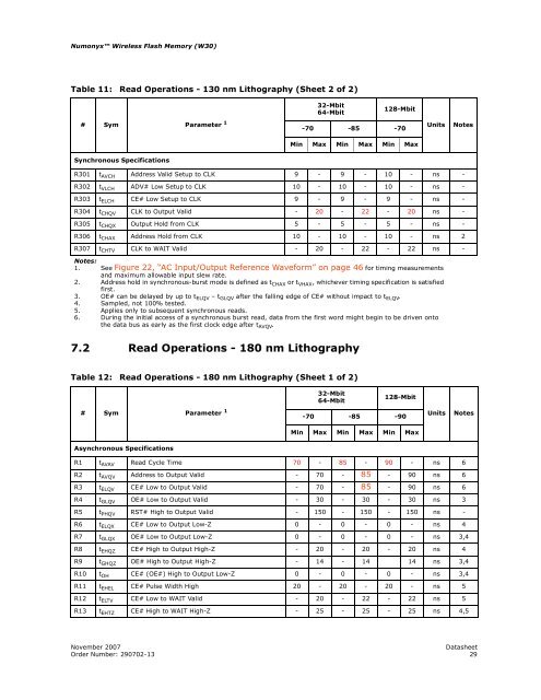
Table 11: Read Operations - 130 nm Lithography (Sheet 2 of 2)<br />
# Sym Parameter 1<br />
Synchronous Specifications<br />
R301 tAVCH Address Valid Setup to CLK 9 - 9 - 10 - ns -<br />
R302 tVLCH ADV# Low Setup to CLK 10 - 10 - 10 - ns -<br />
R303 tELCH CE# Low Setup to CLK 9 - 9 - 9 - ns -<br />
R304 tCHQV CLK to Output Valid - 20 - 22 - 20 ns -<br />
R305 tCHQX Output Hold from CLK 5 - 5 - 5 - ns -<br />
R306 tCHAX Address Hold from CLK 10 - 10 - 10 - ns 2<br />
R307 tCHTV CLK to WAIT Valid - 20 - 22 - 22 ns -<br />
Notes:<br />
1. See Figure 22, “AC Input/Output Reference Waveform” on page 46 for timing measurements<br />
and maximum allowable input slew rate.<br />
2. Address hold in synchronous-burst mode is defined as tCHAX or tVHAX , whichever timing specification is satisfied<br />
first.<br />
3.<br />
4.<br />
OE# can be delayed by up to tELQV – tGLQV after the falling edge of CE# without impact to tELQV. Sampled, not 100% tested.<br />
5. Applies only to subsequent synchronous reads.<br />
6. During the initial access of a synchronous burst read, data from the first word might begin to be driven onto<br />
the data bus as early as the first clock edge after tAVQV. 7.2 Read Operations - 180 nm Lithography<br />
Table 12: Read Operations - 180 nm Lithography (Sheet 1 of 2)<br />
# Sym Parameter 1<br />
Asynchronous Specifications<br />
32-Mbit<br />
64-Mbit<br />
32-Mbit<br />
64-Mbit<br />
128-Mbit<br />
-70 -85 -70<br />
Min Max Min Max Min Max<br />
128-Mbit<br />
-70 -85 -90<br />
Min Max Min Max Min Max<br />
Units Notes<br />
Units Notes<br />
R1 tAVAV Read Cycle Time 70 - 85 - 90 - ns 6<br />
R2 tAVQV Address to Output Valid - 70 - 85 - 90 ns 6<br />
R3 tELQV CE# Low to Output Valid - 70 - 85 - 90 ns 6<br />
R4 tGLQV OE# Low to Output Valid - 30 - 30 - 30 ns 3<br />
R5 tPHQV RST# High to Output Valid - 150 - 150 - 150 ns -<br />
R6 tELQX CE# Low to Output Low-Z 0 - 0 - 0 - ns 4<br />
R7 tGLQX OE# Low to Output Low-Z 0 - 0 - 0 - ns 3,4<br />
R8 tEHQZ CE# High to Output High-Z - 20 - 20 - 20 ns 4<br />
R9 tGHQZ OE# High to Output High-Z - 14 - 14 14 ns 3,4<br />
R10 tOH CE# (OE#) High to Output Low-Z 0 - 0 - 0 - ns 3,4<br />
R11 tEHEL CE# Pulse Width High 20 - 20 - 20 - ns 5<br />
R12 tELTV CE# Low to WAIT Valid - 20 - 22 - 22 ns 5<br />
R13 tEHTZ CE# High to WAIT High-Z - 25 - 25 - 25 ns 4,5<br />
November 2007 Datasheet<br />
Order Number: 290702-13 29