
You also want an ePaper? Increase the reach of your titles
YUMPU automatically turns print PDFs into web optimized ePapers that Google loves.
Numonyx <strong>Wireless</strong> <strong>Flash</strong> <strong>Memory</strong> (<strong>W30</strong>)<br />
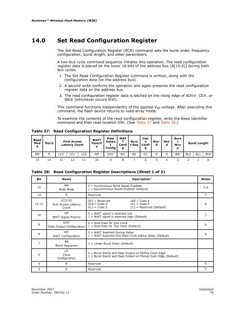
14.0 Set Read Configuration Register<br />
The Set Read Configuration Register (RCR) command sets the burst order, frequency<br />
configuration, burst length, and other parameters.<br />
A two-bus cycle command sequence initiates this operation. The read configuration<br />
register data is placed on the lower 16 bits of the address bus (A[15:0]) during both<br />
bus cycles.<br />
1. The Set Read Configuration Register command is written, along with the<br />
configuration data (on the address bus).<br />
2. A second write confirms the operation and again presents the read configuration<br />
register data on the address bus.<br />
3. The read configuration register data is latched on the rising edge of ADV#, CE#, or<br />
WE# (whichever occurs first).<br />
This command functions independently of the applied V PP voltage. After executing this<br />
command, the flash device returns to read-array mode.<br />
To examine the contents of the read configuration register, write the Read Identifier<br />
command and then read location 05h. (See Table 27 and Table 28.)<br />
Table 27: Read Configuration Register Definitions<br />
Read<br />
Mod<br />
e<br />
Res’d<br />
First Access<br />
Latency Count<br />
WAIT<br />
Polarit<br />
y<br />
Data<br />
Outpu<br />
t<br />
Config<br />
WAI<br />
T<br />
Confi<br />
g<br />
Burs<br />
t Seq<br />
Cloc<br />
k<br />
Confi<br />
g<br />
November 2007 Datasheet<br />
Order Number: 290702-13 79<br />
Res’<br />
d<br />
Res’<br />
d<br />
Burs<br />
t<br />
Wra<br />
p<br />
Burst Length<br />
RM R LC2 LC1 LC0 WP DOC WC BS CC R R BW BL2 BL1 BL0<br />
15 14 13 12 11 10 9 8 7 6 5 4 3 2 1 0<br />
Table 28: Read Configuration Register Descriptions (Sheet 1 of 2)<br />
Bit Name Description1 Notes<br />
15<br />
RM<br />
Read Mode<br />
0 = Synchronous Burst Reads Enabled<br />
1 = Asynchronous Reads Enabled (Default)<br />
14 R Reserved 5<br />
13-11<br />
10<br />
9<br />
8<br />
7<br />
6<br />
LC[2:0]<br />
First Access Latency<br />
Count<br />
WP<br />
WAIT Signal Polarity<br />
DOC<br />
Data Output Configuration<br />
WC<br />
WAIT Configuration<br />
BS<br />
Burst Sequence<br />
CC<br />
Clock<br />
Configuration<br />
001 = Reserved<br />
010 = Code 2<br />
011 = Code 3<br />
0 = WAIT signal is asserted low<br />
1 = WAIT signal is asserted high (Default)<br />
0 = Hold Data for One Clock<br />
1 = Hold Data for Two Clock (Default)<br />
100 = Code 4<br />
101 = Code 5<br />
111 = Reserved (Default)<br />
0 = WAIT Asserted During Delay<br />
1 = WAIT Asserted One Data Cycle before Delay (Default)<br />
1 = Linear Burst Order (Default)<br />
0 = Burst Starts and Data Output on Falling Clock Edge<br />
1 = Burst Starts and Data Output on Rising Clock Edge (Default)<br />
5 R Reserved 5<br />
4 R Reserved 5<br />
2,6<br />
6<br />
3<br />
6<br />
6