A GEM Detector System for an Upgrade of the CMS Muon Endcaps
A GEM Detector System for an Upgrade of the CMS Muon Endcaps
A GEM Detector System for an Upgrade of the CMS Muon Endcaps

Create successful ePaper yourself
Turn your PDF publications into a flip-book with our unique Google optimized e-Paper software.
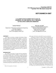
3.3 Single-mask <strong>GEM</strong> production technology<br />
The production <strong>of</strong> <strong>GEM</strong> foils is based on photolithographic techniques commonly used by <strong>the</strong> printed circuit<br />
industry. The copper-clad kapton substrate gets laminated on both sides with solid photoresist <strong>of</strong> 15 µm thickness<br />
that <strong>the</strong> <strong>GEM</strong> hole pattern is tr<strong>an</strong>sferred onto by UV exposure through flexible masks. In order to get good<br />
homogeneity <strong>of</strong> <strong>the</strong> hole geometry across <strong>the</strong> foil, it is very import<strong>an</strong>t to keep <strong>the</strong> alignment error between <strong>the</strong><br />
masks on <strong>the</strong> two <strong>GEM</strong> foil sides within 10 µm. However, since both <strong>the</strong> raw material <strong>an</strong>d <strong>the</strong> two masks are<br />
made from flexible material, <strong>the</strong> m<strong>an</strong>ual alignment procedure becomes extremely cumbersome when <strong>the</strong> linear<br />
dimensions <strong>of</strong> <strong>the</strong> <strong>GEM</strong> exceed 40 cm.<br />
A natural way <strong>of</strong> overcoming this problem is <strong>the</strong> use <strong>of</strong> single-mask photolithography. In this case <strong>the</strong> <strong>GEM</strong> pattern<br />
is tr<strong>an</strong>sferred only to one side <strong>of</strong> <strong>the</strong> raw material, thus removing <strong>an</strong>y need <strong>for</strong> alignment. The exposed photoresist<br />
is developed <strong>an</strong>d <strong>the</strong> hole pattern is used as a mask to chemically etch holes in <strong>the</strong> top copper electrode <strong>of</strong> <strong>the</strong> <strong>GEM</strong><br />
foil. After stripping <strong>the</strong> photoresist, <strong>the</strong> holes in <strong>the</strong> top copper electrode are in turn used as a mask to etch <strong>the</strong><br />
polyimide.<br />
Single-mask photolithography (Fig.10) has been proven to be a valid m<strong>an</strong>ufacturing technique <strong>for</strong> making <strong>GEM</strong>s.<br />
This technology was used to build a prototype detector <strong>for</strong> a possible upgrade <strong>of</strong> <strong>the</strong> TOTEM T1 detector. More<br />
recently, <strong>the</strong> production process has been refined even more, giving great control over <strong>the</strong> dimensions <strong>of</strong> <strong>the</strong> <strong>GEM</strong><br />
holes <strong>an</strong>d <strong>the</strong> size <strong>of</strong> <strong>the</strong> hole rims during <strong>the</strong> production process. Effects <strong>of</strong> <strong>the</strong> hole shape are also being explored<br />
in simulation studies (see below). Production issues have been studied <strong>an</strong>d single-mask <strong>GEM</strong>s are compatible<br />
with industrial production using roll-to-roll equipment, which is a very import<strong>an</strong>t aspect <strong>of</strong> this new technique.<br />
Consequently, a price reduction <strong>for</strong> <strong>GEM</strong> foils is expected from large-scale industrial production that is now<br />
possible.<br />
3.4 Test beam measurements<br />
Figure 10: Overview <strong>of</strong> single-mask etching process <strong>for</strong> <strong>GEM</strong> foils.<br />
The Triple-<strong>GEM</strong> prototypes were tested with a 150 GeV muon/pion beam at <strong>the</strong> CERN SPS H4 beam line during<br />
several RD51 test beam campaigns. The detectors under test were mounted into <strong>the</strong> RD51 Triple-<strong>GEM</strong> beam<br />
telescope as depicted in Figure 11. The telescope itself consists <strong>of</strong> three st<strong>an</strong>dard Triple-<strong>GEM</strong> detectors, referred<br />
to as tracker <strong>GEM</strong>s, each with10cm×10cm active area <strong>an</strong>d running with <strong>an</strong> Ar/CO2 (70:30) gas mixture. They<br />
have 256 strips in both horizontal (y-coordinate) <strong>an</strong>d vertical (x-coordinate) directions tr<strong>an</strong>sverse to <strong>the</strong> beam, with<br />
a pitch <strong>of</strong> 0.4 mm. The telescope detectors were always operated at a gain larger th<strong>an</strong> 10 4 . This setup served as <strong>the</strong><br />
reference tracking device <strong>for</strong> <strong>the</strong> detectors to be tested.<br />
The st<strong>an</strong>dard double-mask Triple-<strong>GEM</strong> prototypes under test were studied with different gas mixtures, Ar/CO2<br />
(70:30, 90:10) <strong>an</strong>d Ar/CO2/CF4 (45:15:40, 60:20:20) at a gas flow <strong>of</strong> about 5 l/hour corresponding to roughly 50<br />
detector volume exch<strong>an</strong>ges per hour. The single-mask Triple-<strong>GEM</strong> was operated with <strong>an</strong> Ar/CO2 mixture only.<br />
The readout <strong>of</strong> all detectors including <strong>the</strong> tracker <strong>GEM</strong>s was done with electronics boards based on VFAT2 (Very<br />
Forward Atlas <strong>an</strong>d Totem) chips [12] developed <strong>for</strong> TOTEM [13] by INFN Siena-Pisa. The VFAT2 ASIC was<br />
designed at CERN using radiation toler<strong>an</strong>t technology. It has a 128-ch<strong>an</strong>nel <strong>an</strong>alog front-end <strong>an</strong>d produces binary<br />
21