A GEM Detector System for an Upgrade of the CMS Muon Endcaps
A GEM Detector System for an Upgrade of the CMS Muon Endcaps
A GEM Detector System for an Upgrade of the CMS Muon Endcaps

You also want an ePaper? Increase the reach of your titles
YUMPU automatically turns print PDFs into web optimized ePapers that Google loves.
VFAT3 The VFAT architecture is <strong>the</strong> baseline front-end ASIC architecture <strong>for</strong> <strong>the</strong> <strong>CMS</strong> <strong>GEM</strong> system. However,<br />
<strong>the</strong> requirements <strong>for</strong> <strong>the</strong> system, whilst very similar to those <strong>of</strong> TOTEM, differ in some very import<strong>an</strong>t ways that<br />
make <strong>the</strong> design <strong>an</strong>d optimization <strong>of</strong> a new front-end ASIC a necessity. The main differences are listed below:<br />
1. Operation at high particle rate using large <strong>GEM</strong> detectors<br />
2. Precise <strong>an</strong>d cle<strong>an</strong> trigger in<strong>for</strong>mation at very high rate (≈2.3MHz/chip)<br />
3. Large detector capacit<strong>an</strong>ce 20 - 60pF<br />
4. Relatively long signal charge collection ≈80ns<br />
5. Interface required : slvds elinks to GBT (as opposed to I 2 C <strong>an</strong>d LVDS)<br />
6. Integrated calibration, bias <strong>an</strong>d monitoring functions,<br />
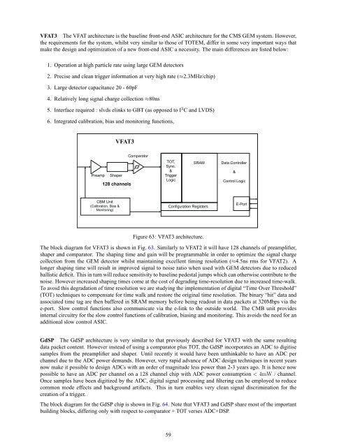
Preamp Shaper<br />
VFAT3<br />
128 ch<strong>an</strong>nels<br />
CBM Unit<br />
(Calibration, Bias &<br />
Monitoring)<br />
Comparator<br />
TOT,<br />
Sync.<br />
&<br />
Trigger<br />
Logic<br />
SRAM<br />
Configuration Registers<br />
Figure 63: VFAT3 architecture.<br />
Data Controller<br />
&<br />
Control Logic<br />
The block diagram <strong>for</strong> VFAT3 is shown in Fig. 63. Similarly to VFAT2 it will have 128 ch<strong>an</strong>nels <strong>of</strong> preamplifier,<br />
shaper <strong>an</strong>d comparator. The shaping time <strong>an</strong>d gain will be programmable in order to optimize <strong>the</strong> signal charge<br />
collection from <strong>the</strong> <strong>GEM</strong> detector whilst maintaining excellent timing resolution (≈4.5ns rms <strong>for</strong> VFAT2). A<br />
longer shaping time will result in improved signal to noise ratio when used with <strong>GEM</strong> detectors due to reduced<br />
ballistic deficit. This in turn will reduce sensitivity to baseline pedestal jumps which c<strong>an</strong> o<strong>the</strong>rwise contribute to <strong>the</strong><br />
noise. However increased shaping times come at <strong>the</strong> cost <strong>of</strong> degrading time-resolution due to increased time-walk.<br />
To avoid this degradation <strong>of</strong> time resolution we are studying <strong>the</strong> implementation <strong>of</strong> digital “Time Over Threshold”<br />
(TOT) techniques to compensate <strong>for</strong> time walk <strong>an</strong>d restore <strong>the</strong> original time resolution. The binary “hit” data <strong>an</strong>d<br />
associated time tag are <strong>the</strong>n buffered in SRAM memory be<strong>for</strong>e being readout in data packets at 320Mbps via <strong>the</strong><br />
e-port. Slow control functions also communicate via <strong>the</strong> e-link to <strong>the</strong> outside world. The CMB unit provides<br />
internal circuitry <strong>for</strong> <strong>the</strong> slow control functions <strong>of</strong> calibration, biasing <strong>an</strong>d monitoring. This avoids <strong>the</strong> need <strong>for</strong> <strong>an</strong><br />
additional slow control ASIC.<br />
GdSP The GdSP architecture is very similar to that previously described <strong>for</strong> VFAT3 with <strong>the</strong> same resulting<br />
data packet content. However instead <strong>of</strong> using a comparator plus TOT, <strong>the</strong> GdSP incorporates <strong>an</strong> ADC to digitise<br />
samples from <strong>the</strong> preamplifier <strong>an</strong>d shaper. Until recently it would have been unthinkable to have <strong>an</strong> ADC per<br />
ch<strong>an</strong>nel due to <strong>the</strong> ADC power dem<strong>an</strong>ds. However, very rapid adv<strong>an</strong>ce <strong>of</strong> ADC design techniques in recent years<br />
now make it possible to design ADCs with <strong>an</strong> order <strong>of</strong> magnitude less power th<strong>an</strong> 2-3 years ago. It is hence now<br />
possible to have <strong>an</strong> ADC per ch<strong>an</strong>nel on a 128 ch<strong>an</strong>nel chip with ADC power consumption < 4mW / ch<strong>an</strong>nel.<br />
Once samples have been digitized by <strong>the</strong> ADC, digital signal processing <strong>an</strong>d filtering c<strong>an</strong> be employed to reduce<br />
common mode effects <strong>an</strong>d background artifacts. This in turn enables very cle<strong>an</strong> signal discrimination <strong>for</strong> <strong>the</strong><br />
creation <strong>of</strong> a trigger.<br />
The block diagram <strong>for</strong> <strong>the</strong> GdSP chip is shown in Fig. 64. Note that VFAT3 <strong>an</strong>d GdSP share most <strong>of</strong> <strong>the</strong> import<strong>an</strong>t<br />
building blocks, differing only with respect to comparator + TOT verses ADC+DSP.<br />
59<br />
E-Port