A GEM Detector System for an Upgrade of the CMS Muon Endcaps
A GEM Detector System for an Upgrade of the CMS Muon Endcaps
A GEM Detector System for an Upgrade of the CMS Muon Endcaps

Create successful ePaper yourself
Turn your PDF publications into a flip-book with our unique Google optimized e-Paper software.
ates <strong>an</strong>d <strong>the</strong> need <strong>for</strong> compatibility with <strong>the</strong> GBT me<strong>an</strong> that a new ASIC will be required <strong>for</strong> <strong>the</strong> future. In <strong>the</strong><br />
following we provide <strong>an</strong> overview <strong>of</strong> <strong>the</strong> VFAT2 chip be<strong>for</strong>e leading on to <strong>the</strong> design requirements <strong>for</strong> a new<br />
front-end chip (VFAT3/GdSP).<br />
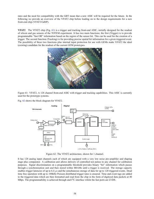
VFAT2 The VFAT2 chip (Fig. 61) is a trigger <strong>an</strong>d tracking front-end ASIC, initially designed <strong>for</strong> <strong>the</strong> readout<br />
<strong>of</strong> silicon <strong>an</strong>d gas sensors <strong>of</strong> <strong>the</strong> TOTEM experiment. It has two main functions; <strong>the</strong> first (Trigger) is to provide<br />
programmable “fast OR” in<strong>for</strong>mation based on <strong>the</strong> region <strong>of</strong> <strong>the</strong> sensor hit. This c<strong>an</strong> be used <strong>for</strong> <strong>the</strong> creation <strong>of</strong> a<br />
trigger. The second function (Tracking) is <strong>for</strong> providing precise spatial hit in<strong>for</strong>mation <strong>for</strong> a given triggered event.<br />
The possibility <strong>of</strong> <strong>the</strong>se two functions plus internal input protection <strong>for</strong> use with <strong>GEM</strong>s make VFAT2 <strong>the</strong> ideal<br />
(existing) c<strong>an</strong>didate <strong>for</strong> <strong>the</strong> readout <strong>of</strong> <strong>the</strong> current <strong>GEM</strong> prototypes.<br />
Figure 61: VFAT2, A 128 ch<strong>an</strong>nel front-end ASIC with trigger <strong>an</strong>d tracking capabilities. This ASIC is currently<br />
used <strong>for</strong> <strong>the</strong> prototype systems.<br />
Fig. 62 shows <strong>the</strong> block diagram <strong>for</strong> VFAT2.<br />
128 ch<strong>an</strong>nels<br />
Analog input<br />
Calibration<br />
Preamp <strong>an</strong>d shaper<br />
DACs<br />
I2C<br />
Receiver <strong>an</strong>d<br />
Registers<br />
SDA SCL<br />
Analog Digital<br />
Comparator<br />
Digital<br />
I/P<br />
Sector<br />
Logic<br />
Sync &<br />
Monostable<br />
SRAM1<br />
Hamming<br />
Enc. & Dec<br />
Control Logic<br />
SRAM2<br />
T1<br />
( LV1A, ReSync, CalPulse, BC0 )<br />
Figure 62: The VFAT2 architecture, shown <strong>for</strong> 1 ch<strong>an</strong>nel.<br />
8 Sector O/Ps<br />
(LVDS)<br />
Data<br />
Formatter<br />
DataOut<br />
(LVDS)<br />
Contains:<br />
Column data<br />
BC<br />
EC<br />
ChipID<br />
CRC<br />
checksum<br />
It has 128 <strong>an</strong>alog input ch<strong>an</strong>nels each <strong>of</strong> which are equipped with a very low noise pre-amplifier <strong>an</strong>d shaping<br />
stage plus comparator. A calibration unit allows delivery <strong>of</strong> controlled test pulses to <strong>an</strong>y ch<strong>an</strong>nel <strong>for</strong> calibration<br />
purposes. Signal discrimination on a programmable threshold provides binary “hit” in<strong>for</strong>mation which passes<br />
through a synchronisation unit <strong>an</strong>d <strong>the</strong>n stored within SRAMs until a trigger is received. The storage capacity<br />
enables trigger latencies <strong>of</strong> up to 6.4 µs <strong>an</strong>d <strong>the</strong> simult<strong>an</strong>eous storage <strong>of</strong> data <strong>for</strong> up to 128 triggered events. Dead<br />
time free operation with up to 100kHz Poisson distributed trigger rates is ensured. Time <strong>an</strong>d event tags are added<br />
to <strong>the</strong> triggered data which are <strong>the</strong>n <strong>for</strong>matted <strong>an</strong>d read from <strong>the</strong> chip in <strong>the</strong> <strong>for</strong>m <strong>of</strong> digitized data packets at 40<br />
Mbps. The programmability is achieved through <strong>an</strong>d I 2 C interface whilst <strong>the</strong> fast ports are LVDS.<br />
58