A GEM Detector System for an Upgrade of the CMS Muon Endcaps
A GEM Detector System for an Upgrade of the CMS Muon Endcaps
A GEM Detector System for an Upgrade of the CMS Muon Endcaps

Create successful ePaper yourself
Turn your PDF publications into a flip-book with our unique Google optimized e-Paper software.
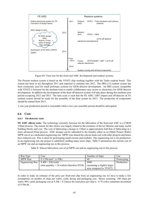
FE ASIC Readout systems<br />
Define electronics system <strong>for</strong> TP,<br />
Formation <strong>of</strong> design teams.<br />
ASIC design to start<br />
Submission <strong>of</strong> FE AISC (VFAT3/<br />
GdSP)<br />
FE ASIC design<br />
team<br />
Approx. 8 m<strong>an</strong><br />
years <strong>of</strong> design<br />
time needed.<br />
2012<br />
2014<br />
2011<br />
From<br />
~ 2014<br />
2015<br />
Present : VFAT2 , Turbo hardware <strong>an</strong>d Labview<br />
DAQ s<strong>of</strong>tware<br />
Medium<br />
term : VFAT2 + SRS<br />
uCTA (<strong>of</strong>f detector<br />
electronics development)<br />
Future : VFAT3/GDSP + GBT + uCTA <strong>of</strong>f<br />
detector electronics.<br />
<strong>System</strong> running with all final components<br />
Figure 69: Time line <strong>for</strong> <strong>the</strong> front-end ASIC development <strong>an</strong>d readout systems.<br />
The Present readout system is based on <strong>the</strong> VFAT2 chip working toge<strong>the</strong>r with <strong>the</strong> Turbo readout board. This<br />
system has been in use throughout 2011 <strong>an</strong>d expected to continue into 2012. The SRS [15] readout system has<br />
been commonly used <strong>for</strong> small prototype systems <strong>for</strong> <strong>GEM</strong> detector development. An SRS system compatible<br />
with VFAT2 is <strong>for</strong>eseen <strong>for</strong> <strong>the</strong> medium term to enable collaborators easy access to electronics <strong>for</strong> <strong>GEM</strong> detector<br />
development. In addition <strong>the</strong> development <strong>of</strong> <strong>the</strong> final <strong>of</strong>f-detector system will take place during this medium term<br />
period occupying 2012 <strong>an</strong>d 2013. The time scale is such that <strong>the</strong> FE ASIC, GBT chipset <strong>an</strong>d <strong>of</strong>f-detector uCTA<br />
readout system should be ready <strong>for</strong> <strong>the</strong> assembly <strong>of</strong> <strong>the</strong> final system by 2015. The production <strong>of</strong> components<br />
should be started from 2015.<br />
A one year production period is reasonable while a two year assembly period should be <strong>an</strong>ticipated.<br />
6.6 Cost:<br />
6.6.1 On-detector costs<br />
FE ASIC silicon costs: The technology currently <strong>for</strong>eseen <strong>for</strong> <strong>the</strong> fabrication <strong>of</strong> <strong>the</strong> front-end ASIC is a CMOS<br />
130nm process. The reason <strong>for</strong> this choice was largely related to <strong>the</strong> existence <strong>of</strong> device libraries <strong>an</strong>d m<strong>an</strong>y useful<br />
building blocks <strong>an</strong>d cost. The cost <strong>of</strong> fabricating a design in 130nm is approximately half that <strong>of</strong> fabricating in a<br />
more adv<strong>an</strong>ced 65nm process. ASIC designs c<strong>an</strong> be submitted to <strong>the</strong> foundry ei<strong>the</strong>r as <strong>an</strong> (Multi Project Wafer)<br />
MPW run or as a dedicated engineering run. MPW runs shared <strong>the</strong> silicon mask cost with o<strong>the</strong>r projects <strong>an</strong>d hence<br />
have reduced cost. This is ideal <strong>for</strong> prototyping small circuits <strong>an</strong>d modules. The engineering run is <strong>for</strong> production.<br />
In <strong>an</strong> engineering run one project is submitted yielding m<strong>an</strong>y more chips. Table 8 summarises <strong>the</strong> current cost <strong>of</strong><br />
<strong>an</strong> MPW run <strong>an</strong>d <strong>an</strong> engineering run in this process.<br />
Table 8: Silicon fabrication cost <strong>of</strong> <strong>an</strong> MPW run <strong>an</strong>d <strong>an</strong> engineering run in this process.<br />
Run Type Cost Number <strong>of</strong> chips Use<br />
MPW Run $ 3.25k/mm 2 , (≈50k) 40 Prototyping<br />
Engineering Run $ 400 + $3k/wafer 6480 Production<br />
(min qu<strong>an</strong>tity = 24 wafers) <strong>the</strong>re<strong>for</strong>e $522k (assuming a slightly larger<br />
area compared to VFAT2)<br />
In order to make <strong>an</strong> estimate <strong>of</strong> <strong>the</strong> price per front-end chip from <strong>an</strong> engineering run we have to make a few<br />
assumptions on number <strong>of</strong> chips per wafer, yield, dicing <strong>an</strong>d packaging cost. Hence assuming 300 chips per<br />
wafer, 90% yield, packaging cost at $ 20k + $ 2/piece <strong>the</strong> total price per chip is $ 78 with a minimum investment<br />
<strong>of</strong> $ 506.4k .<br />
65