

Films minces à base de Si nanostructuré pour des cellules ...
Films minces à base de Si nanostructuré pour des cellules ...
Films minces à base de Si nanostructuré pour des cellules ...

You also want an ePaper? Increase the reach of your titles
YUMPU automatically turns print PDFs into web optimized ePapers that Google loves.
samples from atmosphere since this shoul<strong>de</strong>r lies at the (TO 3 ) <strong>Si</strong>−O peak position.<br />
The inset of gure 4.4 shows that the spectra recor<strong>de</strong>d in the normal inci<strong>de</strong>nce<br />
also exhibits a similar behaviour with annealing. There is a shift of the TO mo<strong>de</strong><br />
between 843-864 cm −1 indicating a rearrangement of the <strong>Si</strong> and N atoms. The TO<br />
peak after CA shows an increased width which is attributed to an overlapping of<br />
TO <strong>Si</strong>−N with (TO 3 ) <strong>Si</strong>−O mo<strong>de</strong>s due to oxidation.<br />
(b) X-Ray Diraction<br />
tel-00916300, version 1 - 10 Dec 2013<br />
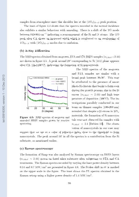
The XRD spectra obtained from as-grown, STA and CA SRSN samples (n 1.95eV =2.44)<br />
are shown in gure 4.5. A peak around 28° corresponding to <strong>Si</strong> (111) plane appears<br />
after CA (1h-1100°C), indicating the formation of <strong>Si</strong> nanocrystals.<br />
The XRD spectra of the as-grown<br />
and STA samples are similar with a<br />
broad peak between 20-30°. This may<br />
be attributed to the presence of amorphous<br />
<strong>Si</strong> clusters that begin to form even<br />
during the growth process, due to the <strong>Si</strong><br />
Figure 4.5: XRD spectra of as-grown and<br />
annealed SRSN samples grown by reactive<br />
sputtering.<br />
excess (n 1.95eV ∼ 2.44) and high temperature<br />
of <strong>de</strong>position (500°C). The investigations<br />
parallely conducted in our<br />
team on thinner samples (100-200 nm)<br />
revealed that <strong>de</strong>spite a <strong>Si</strong> excess in <strong>Si</strong>N x<br />
materials, the formation of <strong>Si</strong> nanocrystals<br />
were not observed for samples with<br />
n 1.95eV < 2.4 [Debieu 12]. The observation<br />
of nanocrystals in our case may<br />
suggest that we are at a value of refractive in<strong>de</strong>x close to the threshold to form<br />
nanocrystals. The peak around 56° in all the spectra is a contribution from the <strong>Si</strong><br />
substrate, as mentioned earlier.<br />
(c) Raman spectroscopy<br />
The formation of <strong>Si</strong>-np was also analyzed by Raman spectroscopy on SRSN layers<br />
(n 1.95eV ∼ 2.44) grown on fused silica substrate after subjecting to STA and CA<br />
treatments. The Raman spectra recor<strong>de</strong>d by varying the laser power <strong>de</strong>nsity between<br />
0.14 and 0.7 MW/cm 2 are presented in gure 4.6. The Stokes shift in eV is marked<br />
on the upper scale in the gure. The inset shows the PL spectra obtained in the<br />
Raman set-up using a higher power <strong>de</strong>nsity of 1.4 MW/cm 2 .<br />
96


