

Films minces à base de Si nanostructuré pour des cellules ...
Films minces à base de Si nanostructuré pour des cellules ...
Films minces à base de Si nanostructuré pour des cellules ...

Create successful ePaper yourself
Turn your PDF publications into a flip-book with our unique Google optimized e-Paper software.
tel-00916300, version 1 - 10 Dec 2013<br />
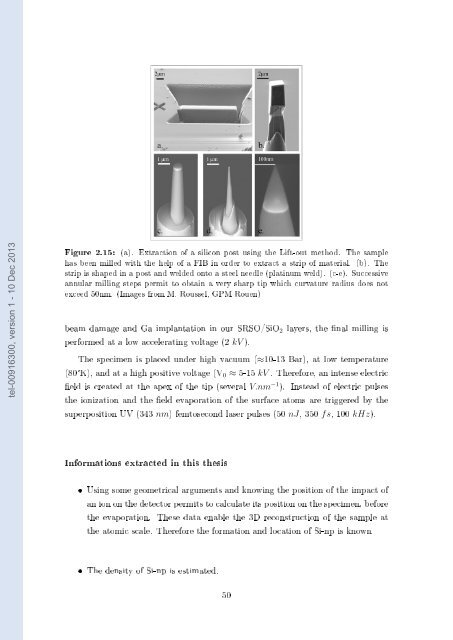
Figure 2.15: (a). Extraction of a silicon post using the Lift-out method. The sample<br />
has been milled with the help of a FIB in or<strong>de</strong>r to extract a strip of material. (b). The<br />
strip is shaped in a post and wel<strong>de</strong>d onto a steel needle (platinum weld). (c-e). Successive<br />
annular milling steps permit to obtain a very sharp tip which curvature radius does not<br />
exceed 50nm. (Images from M. Roussel, GPM Rouen)<br />
beam damage and Ga implantation in our SRSO/<strong>Si</strong>O 2 layers, the nal milling is<br />
performed at a low accelerating voltage (2 kV ).<br />
The specimen is placed un<strong>de</strong>r high vacuum (≈10-13 Bar), at low temperature<br />
(80°K), and at a high positive voltage (V 0 ≈ 5-15 kV . Therefore, an intense electric<br />
eld is created at the apex of the tip (several V.nm −1 ). Instead of electric pulses<br />
the ionization and the eld evaporation of the surface atoms are triggered by the<br />
superposition UV (343 nm) femtosecond laser pulses (50 nJ, 350 fs, 100 kHz).<br />
Informations extracted in this thesis<br />
ˆ Using some geometrical arguments and knowing the position of the impact of<br />
an ion on the <strong>de</strong>tector permits to calculate its position on the specimen, before<br />
the evaporation. These data enable the 3D reconstruction of the sample at<br />
the atomic scale. Therefore the formation and location of <strong>Si</strong>-np is known<br />
ˆ The <strong>de</strong>nsity of <strong>Si</strong>-np is estimated.<br />
50


