

Films minces à base de Si nanostructuré pour des cellules ...
Films minces à base de Si nanostructuré pour des cellules ...
Films minces à base de Si nanostructuré pour des cellules ...

You also want an ePaper? Increase the reach of your titles
YUMPU automatically turns print PDFs into web optimized ePapers that Google loves.
tel-00916300, version 1 - 10 Dec 2013<br />
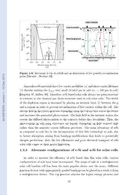
Figure 1.6: Electronic levels of a-<strong>Si</strong>:H and an illustration of few possible recombination<br />
paths [Miroslav , Boehme 10].<br />
Amorphous-<strong>Si</strong> materials have low carrier mobilities (m) and short carrier lifetimes<br />
(t) thereby making the L diff very small (0.1-0.2 mm in a-<strong>Si</strong> vs. ∼ 100 µm in c-<strong>Si</strong>)<br />
[Hegedus 97, Balber 98]. Therefore, a-<strong>Si</strong> <strong>base</strong>d solar cells always use p-i-n structure<br />
in contrast to the classical p-n dio<strong>de</strong> structure used in c-<strong>Si</strong> solar cells. The width<br />
of the <strong>de</strong>pletion region is increased by placing an intrinsic layer (i) between the p<br />
and n regions in or<strong>de</strong>r to prevent recombination of free carriers within the cell. The<br />
electric eld in the i layer increases <strong>de</strong>pending upon the voltage bias across the <strong>de</strong>vice<br />
and increases the generated photocurrent. The high eld in the intrinsic region also<br />
sweeps the diused photocarriers to the contacts before they recombine. Thus, the<br />
photocurrent in a-<strong>Si</strong> p-i-n structures are largely <strong>de</strong>pen<strong>de</strong>nt on eld assisted drift<br />
rather than the minority carrier diusion processes. The main advantage of a-<strong>Si</strong><br />
as compared to c-<strong>Si</strong> lies in the incorporation of thin lm technology to a-<strong>Si</strong>, due<br />
to better absorption arising from bandgap modications that leads to potentially<br />
cheaper production. But, the low eciencies and poor electrical transport of a-<strong>Si</strong><br />
solar cells comes as their major limitation.<br />
1.3.3 Alternate congurations of c-<strong>Si</strong> and a-<strong>Si</strong> for solar cells<br />
In or<strong>de</strong>r to increase the eciency of a-<strong>Si</strong> <strong>base</strong>d thin lm solar cells, various<br />
congurations of a-<strong>Si</strong> have been investigated. The usage of a-<strong>Si</strong> in a multijunction<br />
solar cell/tan<strong>de</strong>m cell has been the most popular choice over the years. Dierent<br />
junction <strong>de</strong>vices with appropriately gra<strong>de</strong>d bandgap can be placed in a stack to form<br />
a multijunction <strong>de</strong>vice. The top junction absorbs the higher energy photons and<br />
12


