Films minces à base de Si nanostructuré pour des cellules ...
Films minces à base de Si nanostructuré pour des cellules ...
Films minces à base de Si nanostructuré pour des cellules ...
Create successful ePaper yourself
Turn your PDF publications into a flip-book with our unique Google optimized e-Paper software.
tel-00916300, version 1 - 10 Dec 2013<br />
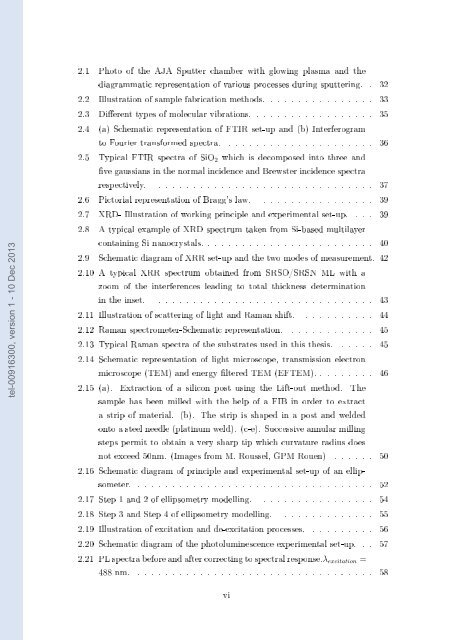
2.1 Photo of the AJA Sputter chamber with glowing plasma and the<br />
diagrammatic representation of various processes during sputtering. . 32<br />
2.2 Illustration of sample fabrication methods. . . . . . . . . . . . . . . . 33<br />
2.3 Dierent types of molecular vibrations. . . . . . . . . . . . . . . . . . 35<br />
2.4 (a) Schematic representation of FTIR set-up and (b) Interferogram<br />
to Fourier transformed spectra. . . . . . . . . . . . . . . . . . . . . . 36<br />
2.5 Typical FTIR spectra of <strong>Si</strong>O 2 which is <strong>de</strong>composed into three and<br />
ve gaussians in the normal inci<strong>de</strong>nce and Brewster inci<strong>de</strong>nce spectra<br />
respectively. . . . . . . . . . . . . . . . . . . . . . . . . . . . . . . . 37<br />
2.6 Pictorial representation of Bragg's law. . . . . . . . . . . . . . . . . 39<br />
2.7 XRD- Illustration of working principle and experimental set-up. . . . 39<br />
2.8 A typical example of XRD spectrum taken from <strong>Si</strong>-<strong>base</strong>d multilayer<br />
containing <strong>Si</strong> nanocrystals. . . . . . . . . . . . . . . . . . . . . . . . . 40<br />
2.9 Schematic diagram of XRR set-up and the two mo<strong>de</strong>s of measurement. 42<br />
2.10 A typical XRR spectrum obtained from SRSO/SRSN ML with a<br />
zoom of the interferences leading to total thickness <strong>de</strong>termination<br />
in the inset. . . . . . . . . . . . . . . . . . . . . . . . . . . . . . . . 43<br />
2.11 Illustration of scattering of light and Raman shift. . . . . . . . . . . 44<br />
2.12 Raman spectrometer-Schematic representation. . . . . . . . . . . . . 45<br />
2.13 Typical Raman spectra of the substrates used in this thesis. . . . . . 45<br />
2.14 Schematic representation of light microscope, transmission electron<br />
microscope (TEM) and energy ltered TEM (EFTEM). . . . . . . . . 46<br />
2.15 (a). Extraction of a silicon post using the Lift-out method. The<br />
sample has been milled with the help of a FIB in or<strong>de</strong>r to extract<br />
a strip of material. (b). The strip is shaped in a post and wel<strong>de</strong>d<br />
onto a steel needle (platinum weld). (c-e). Successive annular milling<br />
steps permit to obtain a very sharp tip which curvature radius does<br />
not exceed 50nm. (Images from M. Roussel, GPM Rouen) . . . . . . 50<br />
2.16 Schematic diagram of principle and experimental set-up of an ellipsometer.<br />
. . . . . . . . . . . . . . . . . . . . . . . . . . . . . . . . . . 52<br />
2.17 Step 1 and 2 of ellipsometry mo<strong>de</strong>lling. . . . . . . . . . . . . . . . . 54<br />
2.18 Step 3 and Step 4 of ellipsometry mo<strong>de</strong>lling. . . . . . . . . . . . . . 55<br />
2.19 Illustration of excitation and <strong>de</strong>-excitation processes. . . . . . . . . . 56<br />
2.20 Schematic diagram of the photoluminescence experimental set-up. . . 57<br />
2.21 PL spectra before and after correcting to spectral response.λ excitation =<br />
488 nm. . . . . . . . . . . . . . . . . . . . . . . . . . . . . . . . . . . 58<br />
vi


