

Films minces à base de Si nanostructuré pour des cellules ...
Films minces à base de Si nanostructuré pour des cellules ...
Films minces à base de Si nanostructuré pour des cellules ...

Create successful ePaper yourself
Turn your PDF publications into a flip-book with our unique Google optimized e-Paper software.
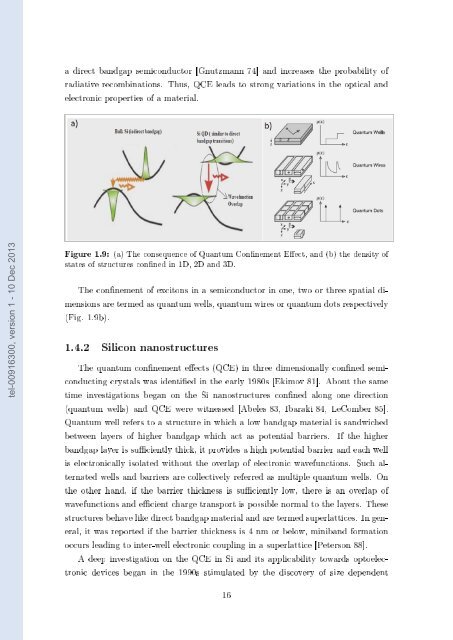
a direct bandgap semiconductor [Gnutzmann 74] and increases the probability of<br />
radiative recombinations. Thus, QCE leads to strong variations in the optical and<br />
electronic properties of a material.<br />
tel-00916300, version 1 - 10 Dec 2013<br />
Figure 1.9: (a) The consequence of Quantum Connement Eect, and (b) the <strong>de</strong>nsity of<br />
states of structures conned in 1D, 2D and 3D.<br />
The connement of excitons in a semiconductor in one, two or three spatial dimensions<br />
are termed as quantum wells, quantum wires or quantum dots respectively<br />
(Fig. 1.9b).<br />
1.4.2 <strong>Si</strong>licon nanostructures<br />
The quantum connement eects (QCE) in three dimensionally conned semiconducting<br />
crystals was i<strong>de</strong>ntied in the early 1980s [Ekimov 81]. About the same<br />
time investigations began on the <strong>Si</strong> nanostructures conned along one direction<br />
(quantum wells) and QCE were witnessed [Abeles 83, Ibaraki 84, LeComber 85].<br />
Quantum well refers to a structure in which a low bandgap material is sandwiched<br />
between layers of higher bandgap which act as potential barriers. If the higher<br />
bandgap layer is suciently thick, it provi<strong>de</strong>s a high potential barrier and each well<br />
is electronically isolated without the overlap of electronic wavefunctions. Such alternated<br />
wells and barriers are collectively referred as multiple quantum wells. On<br />
the other hand, if the barrier thickness is suciently low, there is an overlap of<br />
wavefunctions and ecient charge transport is possible normal to the layers. These<br />
structures behave like direct bandgap material and are termed superlattices. In general,<br />
it was reported if the barrier thickness is 4 nm or below, miniband formation<br />
occurs leading to inter-well electronic coupling in a superlattice [Peterson 88].<br />
A <strong>de</strong>ep investigation on the QCE in <strong>Si</strong> and its applicability towards optoelectronic<br />
<strong>de</strong>vices began in the 1990s stimulated by the discovery of size <strong>de</strong>pen<strong>de</strong>nt<br />
16


