

Films minces à base de Si nanostructuré pour des cellules ...
Films minces à base de Si nanostructuré pour des cellules ...
Films minces à base de Si nanostructuré pour des cellules ...

Create successful ePaper yourself
Turn your PDF publications into a flip-book with our unique Google optimized e-Paper software.
tel-00916300, version 1 - 10 Dec 2013<br />
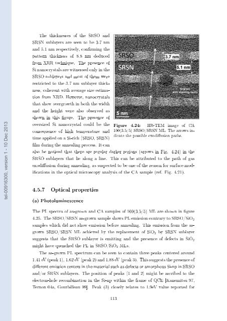
The thicknesses of the SRSO and<br />
SRSN sublayers are seen to be 3.7 nm<br />
and 5.1 nm respectively, conrming the<br />
pattern thickness of 8.8 nm <strong>de</strong>duced<br />
from XRR technique. The presence of<br />
<strong>Si</strong> nanocrystals are witnessed only in the<br />
SRSO sublayers and most of them were<br />
restricted to the 3.7 nm sublayer thickness,<br />
coherent with average size estimation<br />
from XRD. However, nanocrystals<br />
that show overgrowth in both the width<br />
and the height were also observed as<br />
shown in this gure. The presence of<br />
oversized <strong>Si</strong> nanocrystal could be the<br />
consequence of high temperature and<br />
time applied on a <strong>Si</strong>-rich (SRSO, SRSN)<br />
lm during the annealing process. It can<br />
Figure 4.24: HR-TEM image of CA<br />
100(3.5/5) SRSO/SRSN ML. The arrows indicate<br />
the possible exodiusion paths.<br />
also be noticed that there are regular darker regions (arrows in Fig. 4.24) in the<br />
SRSO sublayers that lie along a line. This can be attributed to the path of gas<br />
exodiusion during annealing, as suspected to be one of the reason for surface modications<br />
in the optical microscopy analysis of the CA sample (ref. Fig. 4.21).<br />
4.5.7 Optical properties<br />
(a) Photoluminescence<br />
The PL spectra of as-grown and CA samples of 100(3.5/5) ML are shown in gure<br />
4.25. The SRSO/SRSN as-grown sample shows PL emission contrary to SRSO/<strong>Si</strong>O 2<br />
samples which did not show emission before annealing. This emission from the asgrown<br />
SRSO/SRSN ML achieved by the replacement of <strong>Si</strong>O 2 by SRSN sublayer<br />
suggests that the SRSO sublayer is emitting and the presence of <strong>de</strong>fects in <strong>Si</strong>O 2<br />
might have quenched the PL in SRSO/<strong>Si</strong>O 2 MLs.<br />
The as-grown PL spectrum can be seen to contain three peaks centered around<br />
1.41 eV (peak 1), 1.62 eV (peak 2) and 1.88 eV (peak 3). This suggests the presence of<br />
dierent emission centers in the material such as <strong>de</strong>fects or amorphous <strong>Si</strong>-np in SRSO<br />
and/or SRSN sublayers. The position of peaks (1 and 2) might be ascribed to the<br />
electron-hole recombination in the <strong>Si</strong>-np within the frame of QCE [Kanemitsu 97,<br />
Ternon 04a, Gourbilleau 09]. Peak (3) closely relates to 1.9eV value reported for<br />
113


