

Films minces à base de Si nanostructuré pour des cellules ...
Films minces à base de Si nanostructuré pour des cellules ...
Films minces à base de Si nanostructuré pour des cellules ...

Create successful ePaper yourself
Turn your PDF publications into a flip-book with our unique Google optimized e-Paper software.
The trends of <strong>Si</strong> excess with r H from FTIR is not well <strong>de</strong>ned, but from results<br />
<strong>de</strong>duced from ellipsometry one can notice an increase in the formation of <strong>Si</strong>-np.<br />
3.3 Co-Sputtering- Method 2<br />
tel-00916300, version 1 - 10 Dec 2013<br />
In or<strong>de</strong>r to improve r d and n 1.95eV obtained by reactive sputtering, another method<br />
of incorporating <strong>Si</strong> excess into the <strong>Si</strong>O 2 matrix was adopted. This method involves<br />
co-sputtering of the <strong>Si</strong> and <strong>Si</strong>O 2 targets in a pure Ar plasma at T d =500°C.<br />
The power <strong>de</strong>nsity applied on the <strong>Si</strong> catho<strong>de</strong> was varied to see the inuence on<br />
<strong>de</strong>position rates, refractive in<strong>de</strong>x and structural changes. The power <strong>de</strong>nsity of <strong>Si</strong><br />
can be altered by changing the percentage of the power applied on the <strong>Si</strong> target<br />
with regard to the total power (= 300 W) in the experimental set-up. As before,<br />
the power <strong>de</strong>nsity of <strong>Si</strong>O 2 was xed at 7.4 W/cm 2 while power <strong>de</strong>nsities of <strong>Si</strong> were<br />
varied between 1.62 to 2.96 W/cm 2 .<br />
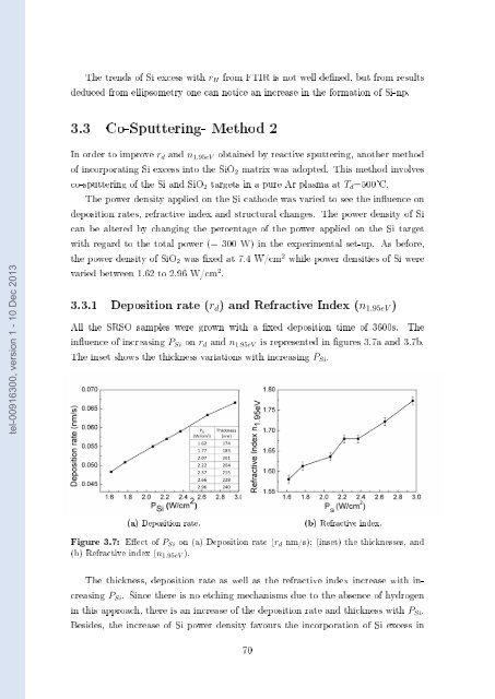
3.3.1 Deposition rate (r d ) and Refractive In<strong>de</strong>x (n 1.95eV )<br />
All the SRSO samples were grown with a xed <strong>de</strong>position time of 3600s. The<br />
inuence of increasing P <strong>Si</strong> on r d and n 1.95eV is represented in gures 3.7a and 3.7b.<br />
The inset shows the thickness variations with increasing P <strong>Si</strong> .<br />
(a) Deposition rate.<br />
(b) Refractive in<strong>de</strong>x.<br />
Figure 3.7: Eect of P <strong>Si</strong> on (a) Deposition rate (r d nm/s); (inset) the thicknesses, and<br />
(b) Refractive in<strong>de</strong>x (n 1.95eV ).<br />
The thickness, <strong>de</strong>position rate as well as the refractive in<strong>de</strong>x increase with increasing<br />
P <strong>Si</strong> . <strong>Si</strong>nce there is no etching mechanisms due to the absence of hydrogen<br />
in this approach, there is an increase of the <strong>de</strong>position rate and thickness with P <strong>Si</strong> .<br />
Besi<strong>de</strong>s, the increase of <strong>Si</strong> power <strong>de</strong>nsity favours the incorporation of <strong>Si</strong> excess in<br />
70


