- Page 2:
SatelliteCommunicationEngineeringMi
- Page 6:
This book is dedicated to my famili
- Page 10:
Because of the immense importance o
- Page 14:
means of a combination of applicati
- Page 18:
about my promise to my students, an
- Page 22:
2.3 Coverage Area and Satellite Net
- Page 26:
1Basic Principles of SatelliteCommu
- Page 30:
and voice (telephone) communication
- Page 34:
FIGURE 1.2Communication between two
- Page 38:
interpreting or uncovering the deci
- Page 42:
cryptographic keys K ti (where i ¼
- Page 46:
FIGURE 1.6Block ciphering technique
- Page 50:
FIGURE 1.7Part of block ciphering w
- Page 54:
Based on the ordering sequence of (
- Page 58:
TABLE 1.1 (continued )S612 1 10 15
- Page 62:
For an uncoded message x and the fe
- Page 66:
2. Your task is to develop a commun
- Page 70:
FIGURE 2.1Geometry of a satellite.
- Page 74:
Future trends in satellite antennas
- Page 78:
In the United States, the three sat
- Page 82:
TABLE 2.3Typical Links Frequency Ba
- Page 86:
FIGURE 2.4Satellite period and orbi
- Page 90:
FIGURE 2.6An illustration of covera
- Page 94:
FIGURE 2.7constellation.A sketch of
- Page 98:
width of 1:73 with reduced coverag
- Page 102:
y ¼ elevation angle of satellite f
- Page 106:
We can conclude that the antenna mu
- Page 110:
FIGURE 2.9Design flowchart of a sat
- Page 114:
Risk control and monitoring measure
- Page 118:
TABLE 2.4Antenna Selection Criteria
- Page 122:
Then the system availability can be
- Page 126:
In fact, MTBF is the reciprocal of
- Page 130:
2.7 ANTENNASBased on function, sate
- Page 134:
Two kinds of horns in common use ar
- Page 138:
FIGURE 2.13Geometry of a parabolic
- Page 142:
FIGURE 2.14 Axisymmetric reflector
- Page 146: A transceiver antenna is a single a
- Page 150: The gain, in the axial mode, of a h
- Page 154: angles, spacecraft may shadow the s
- Page 158: 3. The probability of both parallel
- Page 162: the baseband signal (more details a
- Page 166: matrix in the communications subsys
- Page 170: FIGURE 2.24Typical transfer charact
- Page 174: 4. Iridium LCC (1997). Iridium Syst
- Page 178: 3Earth StationsIn Chap. 2 we discus
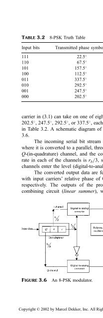
- Page 182: The most popular forms of modulatio
- Page 186: Small earth stations are antennas w
- Page 190: FIGURE 3.2BPSK space diagram.Instea
- Page 194: OQPSKOffset QPSK (OQPSK) is a modif
- Page 200: FIGURE 3.8An M-ary PSK demodulator
- Page 204: where B is the allocated channel ba
- Page 208: A frequently used function is the Q
- Page 212: In view of (3.11), Eq. (3.18) can b
- Page 216: Encoder and DecoderAn encoder is an
- Page 220: Modulator and DemodulatorA modulato
- Page 224: Zero Forcing Technique. Suppose the
- Page 228: The adjoint of matrix A is obtained
- Page 232: FIGURE 3.14The three-tap equalizer
- Page 236: First, in the case of digital signa
- Page 240: than 1=A. Whichever law is used, th
- Page 244: FIGURE 3.16Block diagram for estima
- Page 248:
3.4.2 Antenna TrackingAn earth stat
- Page 252:
controlling antenna pointing. The m
- Page 256:
FIGURE 3.19A generalized model of a
- Page 260:
FIGURE 3.20Entropy of a binary sour
- Page 264:
whereHðYÞ¼output entropy, the av
- Page 268:
To have a feel for this expression,
- Page 272:
2. The system’s overall condition
- Page 276:
transmitted down the fiber as digit
- Page 280:
10. Kantor, L. Y. (ed). (1987). Han
- Page 284:
142. Simulate the probability of bi
- Page 288:
FIGURE 4.1A simplex link.baseband c
- Page 292:
Chapter 2, Sec. 2.7, discusses that
- Page 296:
From (4.6), the received power P r
- Page 300:
FIGURE 4.3A model of the combined-l
- Page 304:
4.1.2 Rain AttenuationRain attenuat
- Page 308:
FIGURE 4.5rates.Average rainstorm p
- Page 312:
FIGURE 4.6Adjacent satellite interf
- Page 316:
FIGURE 4.8Satellite separation dist
- Page 320:
inability of satellite A to accurat
- Page 324:
FIGURE 4.10 Cross-link E b =N 0 vs.
- Page 328:
Then using (4.41), the overall C=N
- Page 332:
(iv)(v)(vi)(vii)Calculate the recei
- Page 336:
5Communication Networks andSystemsC
- Page 340:
discriminate among carriers by temp
- Page 344:
FIGURE 5.2 Principle of FDMA system
- Page 348:
FIGURE 5.3 Operational concept of T
- Page 352:
FIGURE 5.5TDMA: bit rate r b for 1
- Page 356:
Copyright © 2002 by Marcel Dekker,
- Page 360:
5.2 CAPACITY COMPARISON OFMULTIPLE-
- Page 364:
Rearranging (5.11) in terms of ener
- Page 368:
The transmission bit rate isR r ¼
- Page 372:
6Error Detection and CorrectionCodi
- Page 376:
the channel and reconstruct the sou
- Page 380:
message sequence X . Thus, a system
- Page 384:
If we consider a message X ¼ð1010
- Page 388:
can be seen in Table 6.1 that the m
- Page 392:
FIGURE 6.1A (7, 4) cyclic code gene
- Page 396:
FIGURE 6.2Convolutional codes encod
- Page 400:
Alternative methods of describing a
- Page 404:
FIGURE 6.5 Code tree diagram of Fig
- Page 408:
FIGURE 6.8 Code tree diagram of rat
- Page 412:
consistent with the constraint leng
- Page 416:
trellis depth is approximated to 5L
- Page 420:
FIGURE P.1A convolutional coder.the
- Page 424:
7Regulatory Agencies andProceduresT
- Page 428:
of the radiofrequency spectrum, and
- Page 432:
The CCIR works through the medium o
- Page 436:
7.1.3 IFRBThe International Frequen
- Page 440:
The national or regional spectrum m
- Page 444:
3. The need to expand or enhance th
- Page 448:
The DSP will be responsible for res
- Page 452:
2. Provide a convenient framework w
- Page 456:
FIGURE 8.3Types of user-to-network
- Page 460:
H1-channels are designed to carry v
- Page 464:
information. The transfer cell prov
- Page 468:
The OSI layers are divided into two
- Page 472:
plane is denoted by U, the control
- Page 476:
interfacing, maintenance, and conne
- Page 480:
adjoining base station to scan the
- Page 484:
FIGURE 8.9Geometry of a polygon.The
- Page 488:
FIGURE 8.11Splitting cells into sma
- Page 492:
causes signal fading. Of course, th
- Page 496:
FIGURE 8.14TCP=IP suite and its rel
- Page 500:
access to an Internet point of pres
- Page 504:
message security via satellite is d
- Page 508:
REFERENCES1. Wu, W.W. (1989). Eleme
- Page 512:
Appendix ANotationsThe symbols have
- Page 516:
N sPP rP sP TRRðtÞR cR eR rR vSS
- Page 520:
g Central anglez Channel gainZ Ante
- Page 524:
AttenuationBandwidthBearer serviceB
- Page 528:
Frequency divisionmultiple accessFr
- Page 532:
MultiplexingNetworkOmnidirectionala
- Page 536:
UplinkUser-to-networkinterfaceThe e