

Design Challenges: Avoiding the Pitfalls, winning the game - Xilinx
Design Challenges: Avoiding the Pitfalls, winning the game - Xilinx
Design Challenges: Avoiding the Pitfalls, winning the game - Xilinx

Create successful ePaper yourself
Turn your PDF publications into a flip-book with our unique Google optimized e-Paper software.
your most pressing design needs. You will<br />
learn techniques that may allow you to use<br />
a slower speed grade device or fit your<br />
design into a smaller device – ultimately<br />
saving you money. As you master <strong>the</strong> tools<br />
and design methodologies taught in<br />
<strong>Design</strong>ing for Performance, you will be<br />
able to create your design faster, with<br />
increased performance, shortening your<br />
development time and <strong>the</strong>refore costs.<br />
Prerequisites for this course include<br />
Fundamentals of FPGA <strong>Design</strong> and basic<br />
VHDL or Verilog knowledge.<br />
<strong>Design</strong>ing with <strong>the</strong> Virtex-4 Family Course<br />
At this point, you have taken<br />
Fundamentals of FPGA <strong>Design</strong> and<br />
<strong>Design</strong>ing for Performance, but you want<br />
to design into <strong>the</strong> latest and greatest device,<br />
<strong>the</strong> Virtex-4 FPGA. The next course,<br />
<strong>Design</strong>ing with <strong>the</strong> Virtex-4 Family, has an<br />
emphasis on teaching you to obtain <strong>the</strong><br />
highest possible performance (up to 500<br />
MHz internally) and reduce power consumption.<br />
This course covers a myriad of<br />
new and enhanced capabilities of <strong>the</strong><br />
Virtex-4 FPGA fabric, with a major<br />
emphasis on lab exercises.<br />
How do you utilize <strong>the</strong> new DSP48<br />
resource for arithmetic operations? How do<br />
you utilize it for DSP applications? In lab<br />
exercises, you will use <strong>the</strong> DSP48 for DSP<br />
and arithmetic applications requiring 500<br />
MHz operation. Did you know that you<br />
can also use this resource to implement<br />
logic resources such as a 6:1 multiplexer?<br />
We will give you <strong>the</strong> necessary information<br />
to take advantage of this dynamic, highperformance,<br />
and low-power resource.<br />
How would you design a clocking<br />
scheme with ten global clocks and six regional<br />
clocks? In lab exercises, you will use <strong>the</strong><br />
new Xesium clocking resources (see Figure 5)<br />
to design a complex clocking scheme in<br />
Virtex-4 devices. This includes utilizing <strong>the</strong><br />
enhanced DCM, new phase-matched clock<br />
divider (PMCD), enhanced global clock<br />
buffers (BUFGCTRL), and new regional<br />
clocking resources (BUFIO and BUFR).<br />
Have you heard about <strong>the</strong> block RAM<br />
performance enhancements and dedicated<br />
FIFO resources? You will create a 500 MHz<br />
block RAM core employing <strong>the</strong> new<br />
optional output register. You will also create<br />
a core utilizing <strong>the</strong> new dedicated<br />
FIFO16 resources.<br />
Do you need to design a source-synchronous<br />
interface? The new Virtex-4 IOB<br />
tile includes ISERDES and OSERDES<br />
resources. You will examine <strong>the</strong> use of <strong>the</strong><br />
new Xesium clocking resources and <strong>the</strong><br />
ISERDES/OSERDES resources for creating<br />
your own source-synchronous interface.<br />
You will also learn about <strong>the</strong> available<br />
automated tools, ChipSync wizard, and<br />
memory interface generator (MIG) for creating<br />
source-synchronous interfaces.<br />
You will learn to:<br />
• Utilize <strong>the</strong> Xesium global (32) and<br />
regional (2 per region) clock networks<br />
• Dynamically reconfigure <strong>the</strong> DCM’s<br />
frequency syn<strong>the</strong>sized output (CLKFX)<br />
and fine phase shift (DPS)<br />
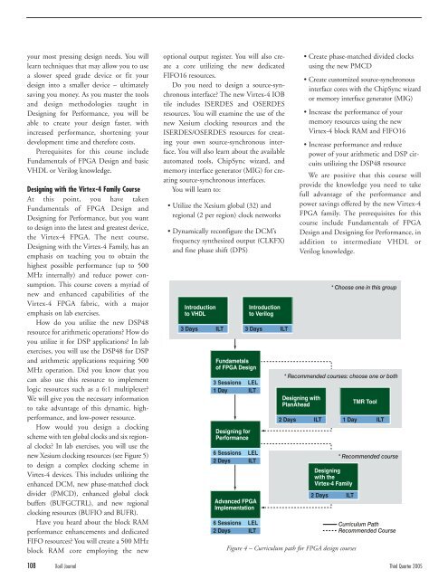
Introduction<br />
to VHDL<br />
3 Days ILT<br />
Fundametals<br />
of FPGA <strong>Design</strong><br />
3 Sessions LEL<br />
1 Day ILT<br />
<strong>Design</strong>ing for<br />
Performance<br />
6 Sessions LEL<br />
2 Days ILT<br />
Advanced FPGA<br />
Implementation<br />
6 Sessions LEL<br />
2 Days ILT<br />
Introduction<br />
to Verilog<br />
3 Days ILT<br />
• Create phase-matched divided clocks<br />
using <strong>the</strong> new PMCD<br />
• Create customized source-synchronous<br />
interface cores with <strong>the</strong> ChipSync wizard<br />
or memory interface generator (MIG)<br />
• Increase <strong>the</strong> performance of your<br />
memory resources using <strong>the</strong> new<br />
Virtex-4 block RAM and FIFO16<br />
• Increase performance and reduce<br />
power of your arithmetic and DSP circuits<br />
utilizing <strong>the</strong> DSP48 resource<br />
We are positive that this course will<br />
provide <strong>the</strong> knowledge you need to take<br />
full advantage of <strong>the</strong> performance and<br />
power savings offered by <strong>the</strong> new Virtex-4<br />
FPGA family. The prerequisites for this<br />
course include Fundamentals of FPGA<br />
<strong>Design</strong> and <strong>Design</strong>ing for Performance, in<br />
addition to intermediate VHDL or<br />
Verilog knowledge.<br />
<strong>Design</strong>ing with<br />
PlanAhead<br />
2 Days ILT<br />
* Choose one in this group<br />
* Recommended courses: choose one or both<br />
<strong>Design</strong>ing<br />
with <strong>the</strong><br />
Virtex-4 Family<br />
2 Days ILT<br />
Figure 4 – Curriculum path for FPGA design courses<br />
TMR Tool<br />
1 Day ILT<br />
* Recommended course<br />
Curriculum Path<br />
Recommended Course<br />
108 Xcell Journal Third Quarter 2005


