

Design Challenges: Avoiding the Pitfalls, winning the game - Xilinx
Design Challenges: Avoiding the Pitfalls, winning the game - Xilinx
Design Challenges: Avoiding the Pitfalls, winning the game - Xilinx

Create successful ePaper yourself
Turn your PDF publications into a flip-book with our unique Google optimized e-Paper software.
Bus Triggering and Display<br />
Traditional oscilloscopes provide digital<br />
triggering capabilities that allow <strong>the</strong>m to<br />
trigger on patterns across analog channels.<br />
With a four-channel oscilloscope, you can<br />
trigger on a single pattern that is as wide as<br />
four signals.<br />
Debug often requires looking at buses<br />
using a specific event as <strong>the</strong> trigger condition.<br />
Using an MSO’s digital channels, you<br />
can trigger on a digital pattern as wide as<br />
16 signals. This can be a powerful capability<br />
if you need to look at a state machine,<br />
an embedded microcontroller, or a data<br />
bus. In addition, you can also trigger<br />
and capture measurements<br />
across all four analog channels,<br />
extending <strong>the</strong> trigger width up to<br />
20 signals, as shown in Figure 1.<br />
Correlating Analog and<br />
Digital Measurements<br />
Although you can use <strong>the</strong> digital<br />
channels to make strictly digital<br />
measurements, <strong>the</strong>ir capabilities<br />
are best employed for looking at<br />
problems that are both functional<br />
and parametric in nature – for<br />
example, triggering on a digital bus<br />
and having this trigger condition<br />
arm <strong>the</strong> scope measurement.<br />
At Agilent, one of our design<br />
teams experienced an infrequent<br />
software glitch on an embedded<br />
product under development. This<br />
anomaly manifested itself very infrequently<br />
– about once a week. The software<br />
team developed diagnostics that<br />
caused <strong>the</strong> problem to happen on a more<br />
frequent basis. With this diagnostic software,<br />
<strong>the</strong>y found that <strong>the</strong> problem<br />
occurred during read cycles on a PCI bus<br />
embedded in an FPGA.<br />
The team routed PCI status signal out<br />
to pins and connected <strong>the</strong> MSO’s digital<br />
channels to <strong>the</strong>se signals. Engineers quickly<br />
set up <strong>the</strong> MSO digital trigger on a PCI<br />
read cycle and <strong>the</strong>n set <strong>the</strong> MSO scope<br />
channels to acquire when <strong>the</strong> MSO digital<br />
channels recorded a PCI bus read cycle.<br />
With <strong>the</strong> ability to trigger on a specific<br />
bus cycle, <strong>the</strong> team was quickly able to<br />
resolve <strong>the</strong> problem. They found a clock<br />
with a too-slow rise time that impacted primarily<br />
read cycles. The team modified <strong>the</strong><br />
design and downloaded a new configuration<br />
file into <strong>the</strong> FPGA. The combination of<br />
reprogrammable FPGAs and MSO measurements<br />
allowed <strong>the</strong> design team to fix <strong>the</strong><br />
problem and ship <strong>the</strong> product on schedule.<br />
Extensive Internal Visibility<br />
To access internal signals, you might typically<br />
use <strong>the</strong> route-out approach to bring signals<br />
to pins that can be probed using an<br />
oscilloscope. Using traditional oscilloscopes,<br />
you would have access to ei<strong>the</strong>r two or four<br />
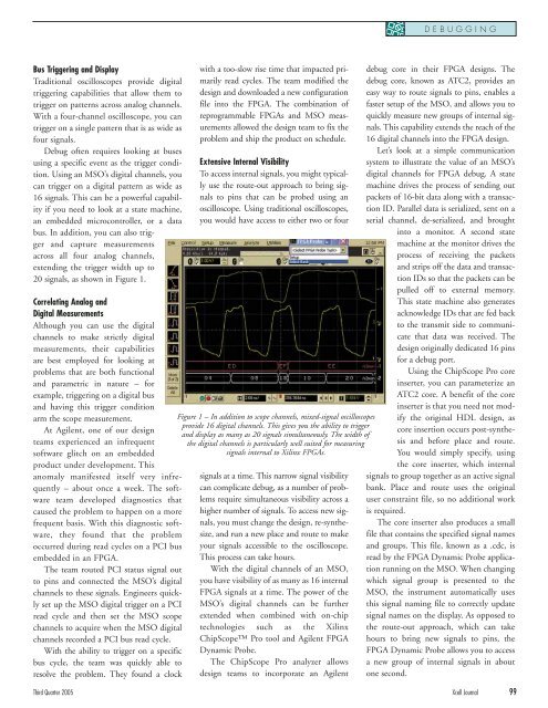
Figure 1 – In addition to scope channels, mixed-signal oscilloscopes<br />
provide 16 digital channels. This gives you <strong>the</strong> ability to trigger<br />
and display as many as 20 signals simultaneously. The width of<br />
<strong>the</strong> digital channels is particularly well suited for measuring<br />
signals internal to <strong>Xilinx</strong> FPGAs.<br />
signals at a time. This narrow signal visibility<br />
can complicate debug, as a number of problems<br />
require simultaneous visibility across a<br />
higher number of signals. To access new signals,<br />
you must change <strong>the</strong> design, re-syn<strong>the</strong>size,<br />
and run a new place and route to make<br />
your signals accessible to <strong>the</strong> oscilloscope.<br />
This process can take hours.<br />
With <strong>the</strong> digital channels of an MSO,<br />
you have visibility of as many as 16 internal<br />
FPGA signals at a time. The power of <strong>the</strong><br />
MSO’s digital channels can be fur<strong>the</strong>r<br />
extended when combined with on-chip<br />
technologies such as <strong>the</strong> <strong>Xilinx</strong><br />
ChipScope Pro tool and Agilent FPGA<br />
Dynamic Probe.<br />
The ChipScope Pro analyzer allows<br />
design teams to incorporate an Agilent<br />
DEBUGGING<br />
debug core in <strong>the</strong>ir FPGA designs. The<br />
debug core, known as ATC2, provides an<br />
easy way to route signals to pins, enables a<br />
faster setup of <strong>the</strong> MSO, and allows you to<br />
quickly measure new groups of internal signals.<br />
This capability extends <strong>the</strong> reach of <strong>the</strong><br />
16 digital channels into <strong>the</strong> FPGA design.<br />
Let’s look at a simple communication<br />
system to illustrate <strong>the</strong> value of an MSO’s<br />
digital channels for FPGA debug. A state<br />
machine drives <strong>the</strong> process of sending out<br />
packets of 16-bit data along with a transaction<br />
ID. Parallel data is serialized, sent on a<br />
serial channel, de-serialized, and brought<br />
into a monitor. A second state<br />
machine at <strong>the</strong> monitor drives <strong>the</strong><br />
process of receiving <strong>the</strong> packets<br />
and strips off <strong>the</strong> data and transaction<br />
IDs so that <strong>the</strong> packets can be<br />
pulled off to external memory.<br />
This state machine also generates<br />
acknowledge IDs that are fed back<br />
to <strong>the</strong> transmit side to communicate<br />
that data was received. The<br />
design originally dedicated 16 pins<br />
for a debug port.<br />
Using <strong>the</strong> ChipScope Pro core<br />
inserter, you can parameterize an<br />
ATC2 core. A benefit of <strong>the</strong> core<br />
inserter is that you need not modify<br />
<strong>the</strong> original HDL design, as<br />
core insertion occurs post-syn<strong>the</strong>sis<br />
and before place and route.<br />
You would simply specify, using<br />
<strong>the</strong> core inserter, which internal<br />
signals to group toge<strong>the</strong>r as an active signal<br />
bank. Place and route uses <strong>the</strong> original<br />
user constraint file, so no additional work<br />
is required.<br />
The core inserter also produces a small<br />
file that contains <strong>the</strong> specified signal names<br />
and groups. This file, known as a .cdc, is<br />
read by <strong>the</strong> FPGA Dynamic Probe application<br />
running on <strong>the</strong> MSO. When changing<br />
which signal group is presented to <strong>the</strong><br />
MSO, <strong>the</strong> instrument automatically uses<br />
this signal naming file to correctly update<br />
signal names on <strong>the</strong> display. As opposed to<br />
<strong>the</strong> route-out approach, which can take<br />
hours to bring new signals to pins, <strong>the</strong><br />
FPGA Dynamic Probe allows you to access<br />
a new group of internal signals in about<br />
one second.<br />
Third Quarter 2005 Xcell Journal 99


