

Design Challenges: Avoiding the Pitfalls, winning the game - Xilinx
Design Challenges: Avoiding the Pitfalls, winning the game - Xilinx
Design Challenges: Avoiding the Pitfalls, winning the game - Xilinx

You also want an ePaper? Increase the reach of your titles
YUMPU automatically turns print PDFs into web optimized ePapers that Google loves.
ages and densities for increased flexibility<br />
and can be gluelessly connected to <strong>the</strong><br />
Spartan-3E FPGA to store any of <strong>the</strong> following:<br />
• Bitstreams for one or more FPGAs<br />
• Boot code, parameters, and data for<br />
soft CPU cores in <strong>the</strong> FPGA<br />
• Multiple bitstreams for <strong>the</strong> same<br />
FPGA utilizing <strong>the</strong> MultiBoot feature<br />
of <strong>the</strong> Spartan-3E device<br />
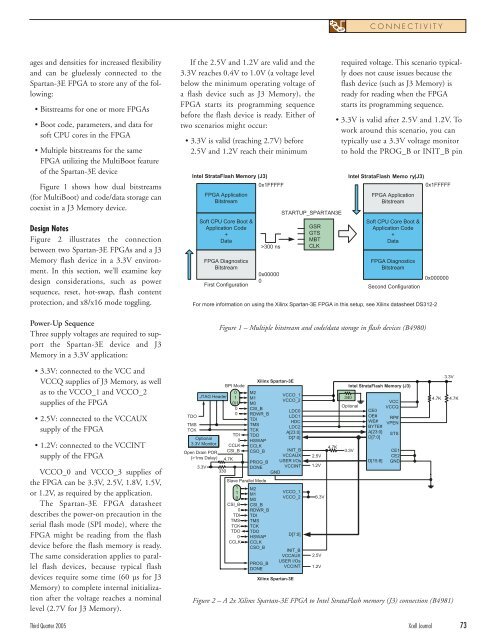
Figure 1 shows how dual bitstreams<br />
(for MultiBoot) and code/data storage can<br />
coexist in a J3 Memory device.<br />
<strong>Design</strong> Notes<br />
Figure 2 illustrates <strong>the</strong> connection<br />
between two Spartan-3E FPGAs and a J3<br />
Memory flash device in a 3.3V environment.<br />
In this section, we’ll examine key<br />
design considerations, such as power<br />
sequence, reset, hot-swap, flash content<br />
protection, and x8/x16 mode toggling.<br />
Power-Up Sequence<br />
Three supply voltages are required to support<br />
<strong>the</strong> Spartan-3E device and J3<br />
Memory in a 3.3V application:<br />
• 3.3V: connected to <strong>the</strong> VCC and<br />
VCCQ supplies of J3 Memory, as well<br />
as to <strong>the</strong> VCCO_1 and VCCO_2<br />
supplies of <strong>the</strong> FPGA<br />
• 2.5V: connected to <strong>the</strong> VCCAUX<br />
supply of <strong>the</strong> FPGA<br />
• 1.2V: connected to <strong>the</strong> VCCINT<br />
supply of <strong>the</strong> FPGA<br />
VCCO_0 and VCCO_3 supplies of<br />
<strong>the</strong> FPGA can be 3.3V, 2.5V, 1.8V, 1.5V,<br />
or 1.2V, as required by <strong>the</strong> application.<br />
The Spartan-3E FPGA datasheet<br />
describes <strong>the</strong> power-on precaution in <strong>the</strong><br />
serial flash mode (SPI mode), where <strong>the</strong><br />
FPGA might be reading from <strong>the</strong> flash<br />
device before <strong>the</strong> flash memory is ready.<br />
The same consideration applies to parallel<br />
flash devices, because typical flash<br />
devices require some time (60 µs for J3<br />
Memory) to complete internal initialization<br />
after <strong>the</strong> voltage reaches a nominal<br />
level (2.7V for J3 Memory).<br />
If <strong>the</strong> 2.5V and 1.2V are valid and <strong>the</strong><br />
3.3V reaches 0.4V to 1.0V (a voltage level<br />
below <strong>the</strong> minimum operating voltage of<br />
a flash device such as J3 Memory), <strong>the</strong><br />
FPGA starts its programming sequence<br />
before <strong>the</strong> flash device is ready. Ei<strong>the</strong>r of<br />
two scenarios might occur:<br />
• 3.3V is valid (reaching 2.7V) before<br />
2.5V and 1.2V reach <strong>the</strong>ir minimum<br />
Intel StrataFlash Memory (J3)<br />
TDO<br />
TMS<br />
TCK<br />
FPGA Application<br />
Bitstream<br />
Soft CPU Core Boot &<br />
Application Code<br />
+<br />
Data<br />
0x1FFFFF<br />
STARTUP_SPARTAN3E<br />
required voltage. This scenario typically<br />
does not cause issues because <strong>the</strong><br />
flash device (such as J3 Memory) is<br />
ready for reading when <strong>the</strong> FPGA<br />
starts its programming sequence.<br />
• 3.3V is valid after 2.5V and 1.2V. To<br />
work around this scenario, you can<br />
typically use a 3.3V voltage monitor<br />
to hold <strong>the</strong> PROG_B or INIT_B pin<br />
FPGA Application<br />
Bitstream<br />
Soft CPU Core Boot &<br />
Application Code<br />
+<br />
Data<br />
FPGA Diagnostics<br />
FPGA Diagnostics<br />
Bitstream<br />
Bitstream<br />
First Configuration<br />
0x00000<br />
0<br />
Second Configuration<br />
0x1FFFFF<br />
0x000000<br />
Third Quarter 2005 Xcell Journal 73<br />
>300 ns<br />
GSR<br />
GTS<br />
MBT<br />
CLK<br />
Intel StrataFlash Memo ry (J3)<br />
For more information on using <strong>the</strong> <strong>Xilinx</strong> Spartan-3E FPGA in this setup, see <strong>Xilinx</strong> datasheet DS312-2<br />
JTAG Header<br />
Optional<br />
3.3V Monitor<br />
Open Drain POR<br />
(>1ms Delay)<br />
3.3V<br />
330<br />
BPI Mode<br />
4.7K<br />
0<br />
1<br />
0/1<br />
0<br />
0<br />
TDI<br />
0<br />
CCLK<br />
CSI_B<br />
1<br />
1<br />
0<br />
CSI_B<br />
0<br />
TDI<br />
TMS<br />
TCK<br />
TDO<br />
0<br />
CCLK<br />
<strong>Xilinx</strong> Spartan-3E<br />
M2<br />
M1<br />
M0<br />
CSI_B<br />
RDWR_B<br />
TDI<br />
TMS<br />
TCK<br />
TDO<br />
HSWAP<br />
CCLK<br />
CSO_B<br />
PROG_B<br />
DONE<br />
Slave Parallel Mode<br />
M2<br />
M1<br />
M0<br />
CSI_B<br />
RDWR_B<br />
TDI<br />
TMS<br />
TCK<br />
TDO<br />
HSWAP<br />
CCLK<br />
CSO_B<br />
PROG_B<br />
DONE<br />
GND<br />
VCCO_1<br />
VCCO_2<br />
LDC0<br />
LDC1<br />
HDC<br />
LDC2<br />
A[23:0]<br />
D[7:0]<br />
INIT_B<br />
VCCAUX<br />
USER I/Os<br />
VCCINT<br />
VCCO_1<br />
VCCO_2<br />
D[7:0]<br />
INIT_B<br />
VCCAUX<br />
USER I/Os<br />
VCCINT<br />
<strong>Xilinx</strong> Spartan-3E<br />
2.5V<br />
1.2V<br />
3.3V<br />
2.5V<br />
1.2V<br />
4.7K<br />
Intel StrataFlash Memory (J3)<br />
340<br />
Optional<br />
3.3V<br />
CONNECTIVITY<br />
Figure 1 – Multiple bitstream and code/data storage in flash devices (B4980)<br />
CE0<br />
OE#<br />
WE#<br />
BYTE#<br />
A[23:0]<br />
D[7:0]<br />
D[15:8]<br />
VCC<br />
VCCQ<br />
RP#<br />
VPEN<br />
STS<br />
CE1<br />
CE2<br />
GND<br />
3.3V<br />
4.7K 4.7K<br />
Figure 2 – A 2x <strong>Xilinx</strong> Spartan-3E FPGA to Intel StrataFlash memory (J3) connection (B4981)


