

Design Challenges: Avoiding the Pitfalls, winning the game - Xilinx
Design Challenges: Avoiding the Pitfalls, winning the game - Xilinx
Design Challenges: Avoiding the Pitfalls, winning the game - Xilinx

Create successful ePaper yourself
Turn your PDF publications into a flip-book with our unique Google optimized e-Paper software.
SYSTEM PERFORMANCE<br />
48-bit result. For example, a “36’b 0101<br />
1111 1111 10101 1101 1110 1111 1000<br />
1110” result would become “48’b 0000<br />
0000 0000 0101 1111 1111 10101 1101<br />
1110 1111 1000 1110”.<br />
Precision Syn<strong>the</strong>sis supports this automatic<br />
sign extension when any of <strong>the</strong><br />
DSP48 operators are inferred. This is a<br />
simple concept, but very powerful, because<br />
it allows you to perform wider arithmetic<br />
operations without having to manually set<br />
<strong>the</strong> correct bus width for <strong>the</strong> output result.<br />
Accumulator (Adder/Subtractor)<br />
The adder/subtractor stages are functions<br />
of <strong>the</strong> inputs, which are driven by <strong>the</strong><br />
upstream multiplexers, carry-select logic,<br />
and multiplier arrays. The CIN, X multiplexer<br />
output, and Y multiplexer output<br />
are always added toge<strong>the</strong>r. You can control<br />
this combined result to be selectively added<br />
to or subtracted from <strong>the</strong> Z multiplexer<br />
output: Adder Out = (Z ± (X + Y + CIN).<br />
Pipeline Registers<br />
This is a unique advantage of <strong>the</strong> DSP48<br />
block compared to o<strong>the</strong>r DSP FPGA architectures.<br />
Each DSP48 slice contains <strong>the</strong><br />
following pipeline registers at each stage:<br />
• One or two pipeline registers for A and<br />
B inputs (AREG and BREG)<br />
• One pipeline register at <strong>the</strong> output<br />
multiplier stage (MREG)<br />
• One pipeline register at <strong>the</strong> output<br />
stage (PREG)<br />
• One pipeline register at <strong>the</strong> C input<br />
• One pipeline register for opmode and<br />
o<strong>the</strong>r control signals<br />
DSP48 Ports<br />
The DSP48 slice input and output ports<br />
support many common DSP and math<br />
algorithms. Two direct 18-bit input data<br />
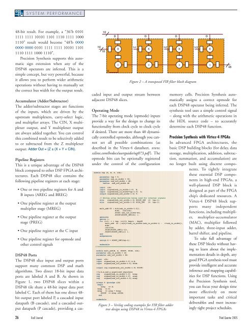
ports are labeled A and B. As shown in<br />
Figure 1, two DSP48 slices within a<br />
DSP48 tile share a 48-bit input data port<br />
labeled C. Each of <strong>the</strong>m has one direct 48bit<br />
output port labeled P, a cascaded input<br />
datapath (B cascade), and a cascaded output<br />
datapath (P cascade), providing a cas-<br />
h0<br />
18<br />
18<br />
0<br />
B<br />
X<br />
+<br />
caded input and output stream between<br />
adjacent DSP48 slices.<br />
Operating Mode<br />
The 7-bit operating mode (opmode) inputs<br />
provide a way for <strong>the</strong> design to change its<br />
functionality from clock cycle to clock cycle<br />
if desired. There are more than 40 dynamically<br />
controlled opmodes, although you cannot<br />
set all possible combinations (as<br />
described in <strong>the</strong> Virtex-4 datasheet, www.<br />
xilinx.com/bvdocs/userguides/ug073.pdf ). The<br />
opmode bits can be optionally registered<br />
under <strong>the</strong> control of <strong>the</strong> configuration<br />
module top (h, B, P, clk);<br />
parameter tap = 4;<br />
parameter sub_in_width = 18;<br />
parameter sub_out_width = 48;<br />
`define sub_out_width 48<br />
h1<br />
input clk;<br />
input signed[sub_in_width-1:0] B;<br />
input signed[sub_in_width*tap-1:0] h;<br />
output signed[sub_out_width-1:0] P;<br />
// Wiring array declarations being used for internal signals<br />
wire signed[sub_out_width-1:0] PCOUT_INT [0: tap-1];<br />
wire signed[sub_out_width-1:0] PCIN_INT [0: tap-1];<br />
mult_add U0 (.A(h[sub_in_width-1:0]),<br />
.B(B), .clk(clk),<br />
.PCIN(`sub_out_width'b0),<br />
.PCOUT(PCOUT_INT[0]) );<br />
generate<br />
genvar i;<br />
for (i=1; i < tap; i=i+1) begin : dsp48<br />
mult_add UI (.A(h[i*sub_in_width+(sub_in_width-1) : i*sub_in_width]),<br />
.B(B),<br />
.clk(clk),<br />
.PCIN(PCOUT_INT[i-1]),<br />
.PCOUT(PCOUT_INT[i]) );<br />
end<br />
endgenerate<br />
assign P = PCOUT_INT[tap-1];<br />
endmodule<br />
//========================================<br />
module mult_add(B, A, PCOUT, PCIN, clk);<br />
parameter sub_in_width = 18;<br />
parameter sub_out_width = 48;<br />
input clk;<br />
input signed[sub_in_width-1:0] A,B;<br />
input signed[sub_out_width-1:0] PCIN;<br />
output reg signed[sub_out_width-1:0] PCOUT;<br />
//a,b,m,and p pipelined registers<br />
reg signed[sub_in_width-1:0] breg;<br />
reg signed[sub_in_width-1:0] areg;<br />
reg signed[sub_out_width-1:0] mreg;<br />
always @ (posedge clk)<br />
begin<br />
areg


