

Design Challenges: Avoiding the Pitfalls, winning the game - Xilinx
Design Challenges: Avoiding the Pitfalls, winning the game - Xilinx
Design Challenges: Avoiding the Pitfalls, winning the game - Xilinx

Create successful ePaper yourself
Turn your PDF publications into a flip-book with our unique Google optimized e-Paper software.
Pblocks can direct <strong>the</strong> flow of <strong>the</strong><br />
design based on <strong>the</strong> connectivity of<br />
different modules. The connectivity<br />
of <strong>the</strong> I/Os to and between modules is<br />
shown for <strong>the</strong> placed and routed<br />
design through net bundles. We create<br />
Pblocks to cover <strong>the</strong> critical paths,<br />
which are usually associated with getting<br />
on or off <strong>the</strong> device.<br />
The schematic view also displays<br />
<strong>the</strong> connectivity of <strong>the</strong> design (Figure<br />
2). Pblocks are created ei<strong>the</strong>r in <strong>the</strong><br />
device, schematic, or netlist views.<br />
The critical paths and o<strong>the</strong>r timing<br />
paths relative to <strong>the</strong> existing floorplanning<br />
can be highlighted in <strong>the</strong><br />
device and schematic views.<br />
Normally, <strong>the</strong> schematic view is<br />
used to examine <strong>the</strong> critical modules<br />
and paths without worrying about <strong>the</strong><br />
actual placement of those modules.<br />
The congestion around existing<br />
Pblocks and <strong>the</strong> resource utilization<br />
of a Pblock are seen in <strong>the</strong> device<br />
view. If <strong>the</strong> timing is critical within<br />
<strong>the</strong> Pblock (indicated by a high<br />
resource utilization count) <strong>the</strong>n we<br />
resize <strong>the</strong> Pblock to give <strong>the</strong> congested<br />
logic more room to meet timing by<br />
condensing <strong>the</strong> logic to shorten <strong>the</strong><br />
interconnect lengths and delays. We<br />
can also move <strong>the</strong> Pblocks to alleviate<br />
congestion or merge congested logic<br />
into a single Pblock.<br />
We create and place <strong>the</strong> Pblocks, <strong>the</strong>n<br />
run place and route with our floorplanning<br />
constraints. We also lock <strong>the</strong> locations of <strong>the</strong><br />
larger components and critical logic, which<br />
includes block RAMs, DSP48s, and DCMs.<br />
Then we run place and route on <strong>the</strong> design<br />
and repeat <strong>the</strong> process by reviewing <strong>the</strong> timing<br />
report and placement of <strong>the</strong> design and<br />
modifying <strong>the</strong> constraints (Figure 2). We<br />
can also create smaller “child” Pblocks inside<br />
o<strong>the</strong>r Pblocks to help <strong>the</strong> grouping of a few<br />
components for timing-critical paths.<br />
Place and route is run on individual<br />
Pblocks in addition to <strong>the</strong> entire design.<br />
This helps determine if timing can be met<br />
inside <strong>the</strong> module or Pblock without affecting<br />
<strong>the</strong> rest of <strong>the</strong> design. If we are unable<br />
to meet timing on a specific Pblock, we go<br />
back to <strong>the</strong> source code and re-write it.<br />
Figure 1 – Timing analysis and placement<br />
view of a sample design<br />
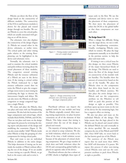
Figure 2 – <strong>Design</strong> connectivity in <strong>the</strong><br />
schematic view and timing analysis with<br />
<strong>the</strong> larger components placed<br />
PlanAhead software can import <strong>the</strong><br />
updated netlist for any module and keep<br />
<strong>the</strong> Pblocks originally created. After meeting<br />
timing requirements, we place location<br />
constraints on all of <strong>the</strong> elements of that<br />
Pblock. This helps ensure that timing is<br />
retained when <strong>the</strong> rest of <strong>the</strong> design is<br />
placed and routed.<br />
The majority of timing failures that we<br />
see are related to setup violations. We also<br />
see hold violations, which are tricky to fix.<br />
Most of <strong>the</strong> time, a hold violation occurs<br />
because of <strong>the</strong> placement of critical clocking<br />
components. We get a large number of<br />
clock skew and hold violations when <strong>the</strong><br />
DCM and corresponding global buffer are<br />
placed on opposite sides of <strong>the</strong> device.<br />
PlanAhead software also has a robust set<br />
of DRC checks to highlight <strong>the</strong>se types of<br />
SYSTEM PERFORMANCE<br />
issues early in <strong>the</strong> flow. We use <strong>the</strong><br />
schematic and device views to view<br />
<strong>the</strong> placement of <strong>the</strong>se components.<br />
We <strong>the</strong>n move <strong>the</strong> placement of<br />
ei<strong>the</strong>r <strong>the</strong> DCM or <strong>the</strong> global buffer<br />
so that <strong>the</strong>se components are near<br />
each o<strong>the</strong>r.<br />
The <strong>Design</strong> Doesn’t Fit<br />
When a design has difficulty fitting<br />
into <strong>the</strong> target device, we run it without<br />
any floorplanning constraints.<br />
Usually, overlapping Pblocks exist,<br />
which we remove. We place <strong>the</strong> large<br />
components manually, as we described<br />
in <strong>the</strong> previous section, to help <strong>the</strong><br />
place and route tools.<br />
If timing is not a critical issue for<br />
this design, we <strong>the</strong>n create Pblocks<br />
of <strong>the</strong> major hierarchical blocks of<br />
<strong>the</strong> design. The Pblocks are used to<br />
direct <strong>the</strong> flow of <strong>the</strong> design based<br />
on connectivity of <strong>the</strong> module with<br />
net bundles. The bundles show <strong>the</strong><br />
amount of connectivity based on <strong>the</strong><br />
size of <strong>the</strong> bundle. We place <strong>the</strong><br />
Pblocks close to <strong>the</strong> components<br />
that drive <strong>the</strong>m based on <strong>the</strong> net<br />
bundles and Pblock statistics. We<br />
also place <strong>the</strong> entire design into a<br />
Pblock and use <strong>the</strong> compression<br />
attribute on <strong>the</strong> Pblock(s) to tell<br />
MAP to pack this portion of <strong>the</strong><br />
design as tight as possible. This<br />
attribute opens up more room on <strong>the</strong> rest<br />
of <strong>the</strong> device for <strong>the</strong> remaining logic, but<br />
has a negative effect on timing.<br />
We also run place and route on <strong>the</strong><br />
individual Pblocks of <strong>the</strong> design. This<br />
helps ensure that <strong>the</strong> logic placed in <strong>the</strong><br />
Pblocks can be placed and routed within<br />
<strong>the</strong> defined Pblock size and eventually in<br />
<strong>the</strong> device specified. We can manually<br />
compress <strong>the</strong> size of <strong>the</strong> Pblock until MAP<br />
fails. Once MAP fails, we revert back to<br />
<strong>the</strong> last known good size of <strong>the</strong> Pblock.<br />
The statistics of <strong>the</strong> Pblock may<br />
report that we used more than 100%,<br />
but MAP will determine if it passes. We<br />
repeat this process if o<strong>the</strong>r non-timing<br />
critical Pblocks exist and use <strong>the</strong> compression<br />
attribute to pack those Pblocks<br />
as tight as possible.<br />
Third Quarter 2005 Xcell Journal 21


