

Design Challenges: Avoiding the Pitfalls, winning the game - Xilinx
Design Challenges: Avoiding the Pitfalls, winning the game - Xilinx
Design Challenges: Avoiding the Pitfalls, winning the game - Xilinx

Create successful ePaper yourself
Turn your PDF publications into a flip-book with our unique Google optimized e-Paper software.
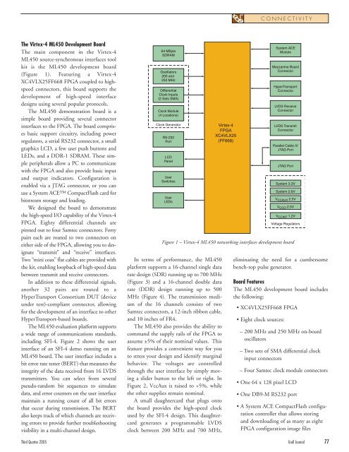
The Virtex-4 ML450 Development Board<br />
The main component in <strong>the</strong> Virtex-4<br />
ML450 source-synchronous interfaces tool<br />
kit is <strong>the</strong> ML450 development board<br />
(Figure 1). Featuring a Virtex-4<br />
XC4VLX25FF668 FPGA coupled to highspeed<br />
connectors, this board supports <strong>the</strong><br />
development of high-speed interface<br />
designs using several popular protocols.<br />
The ML450 demonstration board is a<br />
simple board providing several connector<br />
interfaces to <strong>the</strong> FPGA. The board comprises<br />
basic support circuitry, including power<br />
regulators, a serial RS232 connector, a small<br />
graphics LCD, a few user push buttons and<br />
LEDs, and a DDR-1 SDRAM. These simple<br />
peripherals allow a PC to communicate<br />
with <strong>the</strong> FPGA and also provide basic input<br />
and output indicators. Configuration is<br />
enabled via a JTAG connector, or you can<br />
use a System ACE CompactFlash card for<br />
bitstream storage and loading.<br />
We designed <strong>the</strong> board to demonstrate<br />
<strong>the</strong> high-speed I/O capability of <strong>the</strong> Virtex-4<br />
FPGA. Eighty differential channels are<br />
pinned out to four Samtec connectors. Forty<br />
pairs each are routed to two connectors on<br />
ei<strong>the</strong>r side of <strong>the</strong> FPGA, allowing you to designate<br />
“transmit” and “receive” interfaces.<br />
Two “mini coax” flat cables are provided with<br />
<strong>the</strong> kit, enabling loopback of high-speed data<br />
between transmit and receive connectors.<br />
In addition to <strong>the</strong>se differential signals,<br />
ano<strong>the</strong>r 32 pairs are routed to a<br />
HyperTransport Consortium DUT (device<br />
under test)-compliant connector, allowing<br />
for <strong>the</strong> development of an interface to o<strong>the</strong>r<br />
HyperTransport-based boards.<br />
The ML450 evaluation platform supports<br />
a wide range of communications standards,<br />
including SFI-4. Figure 2 shows <strong>the</strong> user<br />
interface of an SFI-4 demo running on an<br />
ML450 board. The user interface includes a<br />
bit error rate tester (BERT) that measures <strong>the</strong><br />
integrity of <strong>the</strong> data received from 16 LVDS<br />
transmitters. You can select from several<br />
pseudo-random bit sequences to simulate<br />
data, and error counters on <strong>the</strong> user interface<br />
maintain a running count of all bit errors<br />
that occur during transmission. The BERT<br />
also keeps track of which channels are receiving<br />
errors to provide fur<strong>the</strong>r troubleshooting<br />
visibility in a multi-channel design.<br />
64 MByte<br />
SDRAM<br />
Oscillators<br />
200 and<br />
250 MHz<br />
Differential<br />
Clock Inputs<br />
(2 Sets SMA)<br />
Clock Module<br />
(4 Locations)<br />
Clock Generator<br />
RS-232<br />
Port<br />
LCD<br />
Panel<br />
User<br />
Switches<br />
User<br />
LEDs<br />
In terms of performance, <strong>the</strong> ML450<br />
platform supports a 16-channel single data<br />
rate design (SDR) running up to 700 MHz<br />
(Figure 3) and a 16-channel double data<br />
rate (DDR) design running up to 500<br />
MHz (Figure 4). The transmission medium<br />
of <strong>the</strong> 16 channels consists of two<br />
Samtec connectors, a 12-inch ribbon cable,<br />
and 10 inches of FR4.<br />
The ML450 also provides <strong>the</strong> ability to<br />
command <strong>the</strong> supply rails of <strong>the</strong> FPGA to<br />
assume ±5% of <strong>the</strong>ir nominal values. This<br />
feature provides a convenient way for you<br />
to stress your design and identify marginal<br />
behavior. The voltages are controlled<br />
through <strong>the</strong> user interface by simply moving<br />
a slider button to <strong>the</strong> left or right. In<br />
Figure 2, VccAux is raised to +5%, while<br />
<strong>the</strong> o<strong>the</strong>r supplies remain nominal.<br />
A small daughtercard that plugs onto<br />
<strong>the</strong> board provides <strong>the</strong> high-speed clock<br />
used by <strong>the</strong> SFI-4 design. This daughtercard<br />
generates a programmable LVDS<br />
clock between 200 MHz and 700 MHz,<br />
Virtex-4<br />
FPGA<br />
XC4VLX25<br />
(FF668)<br />
CONNECTIVITY<br />
eliminating <strong>the</strong> need for a cumbersome<br />
bench-top pulse generator.<br />
Board Features<br />
The ML450 development board includes<br />
<strong>the</strong> following:<br />
• XC4VLX25FF668 FPGA<br />
• Eight clock sources:<br />
System ACE<br />
Module<br />
Mezzanine Board<br />
Connector<br />
HyperTransport<br />
Connector<br />
LVDS Receive<br />
Connector<br />
LVDS Transmit<br />
Connector<br />
Parallel Cable IV<br />
JTAG Port<br />
JTAG Port<br />
System 3.3V<br />
System 2.6V<br />
VCCAUX 2.5V<br />
V CCO 2.5V<br />
V CCINT 1.2V<br />
Voltage Regulators<br />
Figure 1 – Virtex-4 ML450 networking interfaces development board<br />
– 200 MHz and 250 MHz on-board<br />
oscillators<br />
– Two sets of SMA differential clock<br />
input connectors<br />
– Four Samtec clock module connectors<br />
• One 64 x 128 pixel LCD<br />
• One DB9-M RS232 port<br />
• A System ACE CompactFlash configuration<br />
controller that allows storing<br />
and downloading of as many as eight<br />
FPGA configuration image files<br />
Third Quarter 2005 Xcell Journal 77


