

Design Challenges: Avoiding the Pitfalls, winning the game - Xilinx
Design Challenges: Avoiding the Pitfalls, winning the game - Xilinx
Design Challenges: Avoiding the Pitfalls, winning the game - Xilinx

Create successful ePaper yourself
Turn your PDF publications into a flip-book with our unique Google optimized e-Paper software.
CONNECTIVITY<br />
In this article, I’ll address <strong>the</strong> third reason<br />
in detail. Although my focus is on<br />
<strong>Xilinx</strong> ® Virtex-II Pro RocketIO technology,<br />
<strong>the</strong> information would apply to<br />
any serial interface, including RocketIO<br />
transceivers in Virtex-4 devices.<br />
Line Loss<br />
An ideal lossless transmission line assumes<br />
that a signal propagates down <strong>the</strong> line with<br />
no energy loss. In o<strong>the</strong>r words, if a 1.0V<br />
signal with a 1.0 ns rise time enters one end<br />
of <strong>the</strong> line, <strong>the</strong> same 1.0V and 1.0 ns signal<br />
will come out <strong>the</strong> far end.<br />
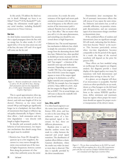
Figure 1 – Reciever waveforms for a lossless line,<br />
as well as 10, 20, and 40 in lines, showing<br />
both attenuation and rise-time degradation<br />
for a 2 GHz signal. (Simulated with Mentor<br />
Graphics HyperLynx.)<br />
This is a good approximation when signal<br />
rise times are on <strong>the</strong> order of 1.0 ns (or<br />
slower), and with trace lengths of 10 in (or<br />
shorter). However, as rise times trend<br />
toward 100 ps and lengths get significantly<br />
longer (as in a backplane), <strong>the</strong> lossy effects<br />
of transmission lines begin to influence signal<br />
quality dramatically. As Figure 1 shows,<br />
<strong>the</strong>se effects – both attenuation and risetime<br />
degradation – vary directly with<br />
length at higher frequencies.<br />
To describe and accurately predict <strong>the</strong><br />
behavior of real interconnects, two important<br />
mechanisms that absorb energy from<br />
<strong>the</strong> signal must be modeled:<br />
• Resistive loss. From DC through frequencies<br />
up to a few megahertz, <strong>the</strong><br />
current in a trace moves through <strong>the</strong><br />
entire cross-sectional area of <strong>the</strong> trace.<br />
At higher frequencies, however, current<br />
flows along <strong>the</strong> perimeter of a line<br />
ra<strong>the</strong>r than uniformly across <strong>the</strong> entire<br />
cross-section. As a result, <strong>the</strong> series<br />
resistance of <strong>the</strong> signal and return path<br />
conductors increases with <strong>the</strong> square<br />
root of frequency as <strong>the</strong> effective crosssection<br />
of <strong>the</strong> interconnect path is<br />
reduced. Resistive loss is also referred<br />
to as “skin effect.” But no matter what<br />
you call it, it is <strong>the</strong> same phenomenon,<br />
and something you should be concerned<br />
about at high frequencies.<br />
• Dielectric loss. The second important<br />
loss mechanism is dielectric loss, which<br />
is simply <strong>the</strong> conversion of electrical<br />
energy from <strong>the</strong> alternating electric field<br />
into heat. Dielectric loss, often specified<br />
in decibels per meter, increases with frequency<br />
and varies inversely with a material’s<br />
“loss tangent” – a function of <strong>the</strong><br />
material’s resin type and molecular<br />
structure. Depending on resin content,<br />
“vanilla” FR-4 has a loss tangent ranging<br />
from 0.02-0.03. Lower loss tangent<br />
equates to more of <strong>the</strong> output signal<br />
getting to its destination, as well as<br />
higher material costs compared to FR-4.<br />
GETEK, for example, has a loss tangent<br />
of 0.012. Nelco 4000-13 is 0.01. And<br />
<strong>the</strong> loss tangent for Rogers 4003 is as<br />
low as 0.0027. For an actual design, you<br />
will want to discuss <strong>the</strong> tradeoffs with<br />
your board vendor.<br />
Loss, Jitter, and ISI<br />
I’ve often heard engineers use<br />
<strong>the</strong> terms inter-symbol interference<br />
(ISI), jitter, and loss<br />
to refer to <strong>the</strong> same thing: <strong>the</strong><br />
unknown cause of a lessthan-optimal<br />
signal or bitstream.<br />
In fact, <strong>the</strong>se are<br />
different phenomena.<br />
Random jitter is used to<br />
describe random events that<br />
result in a delay between <strong>the</strong><br />
expected and actual signal<br />
transition. The distribution of<br />
random effects follows a classic<br />
Gaussian distribution, where<br />
<strong>the</strong> results vary wider (in time)<br />
as more data is observed. This<br />
data is typically provided by<br />
<strong>the</strong> driver manufacturer.<br />
Deterministic jitter encompasses <strong>the</strong><br />
list of systematic interconnect effects that<br />
will reoccur if you repeat <strong>the</strong> same stimulus.<br />
Dielectric and resistive loss, as well as<br />
crosstalk, reflections, via parasitics, returnpath<br />
discontinuities, and any systematic<br />
aspect of an interconnect design contribute<br />
to deterministic jitter.<br />
If <strong>the</strong> combined effects of random and<br />
deterministic jitter are significant enough,<br />
ISI will result, indicating that bit distinctions<br />
have become “blurry” at <strong>the</strong> receiver.<br />
This becomes particularly serious<br />
when rise-time degradation becomes<br />
comparable to <strong>the</strong> bit period of <strong>the</strong> signal.<br />
As a result, <strong>the</strong> shape of <strong>the</strong> received<br />
waveform will depend on <strong>the</strong> prior bit<br />
pattern (ISI).<br />
These effects are best modeled using<br />
an oscilloscope that supports eye diagram<br />
analysis. Eye diagrams provide a visual<br />
display of <strong>the</strong> signal quality over many bit<br />
transitions with both deterministic and<br />
random jitter serving to close <strong>the</strong> “eye.”<br />
At a glance, an eye diagram will show<br />
if an interconnect is acceptable. Pass/fail<br />
criteria are often specified by an eye mask,<br />
shown as a blue hexagon on <strong>the</strong> left-hand<br />
side of Figure 2. Eye masks, which conform<br />
to <strong>the</strong> various SERDES specifications,<br />
define minimum and maximum<br />
keep-out regions where proper bit transitions<br />
should not appear for proper receiver<br />
interpretation of <strong>the</strong> driver’s intent.<br />
Figure 2 – The eye shows encroachment on <strong>the</strong> XAUI eye mask<br />
when using 10% pre-emphasis for a 36 in FR-4 transmission<br />
path with four vias and two Teradyne VHDM-HSD5 connectors<br />
(simulated with HyperLynx LineSim GHz).<br />
70 Xcell Journal Third Quarter 2005


