

Design Challenges: Avoiding the Pitfalls, winning the game - Xilinx
Design Challenges: Avoiding the Pitfalls, winning the game - Xilinx
Design Challenges: Avoiding the Pitfalls, winning the game - Xilinx

Create successful ePaper yourself
Turn your PDF publications into a flip-book with our unique Google optimized e-Paper software.
Controlling Noise<br />
A well-designed package is critical to signal<br />
integrity. Noise can emanate from<br />
many sources in a system. If <strong>the</strong> noise<br />
source is on <strong>the</strong> board, <strong>the</strong>re are some<br />
potential solutions once you find out<br />
where <strong>the</strong> problem is (probably after a<br />
long and laborious debug process). If <strong>the</strong><br />
problem is in <strong>the</strong> package, you have little<br />
or no choice but to change <strong>the</strong> design,<br />
vendor, or parts. This is a time-consuming<br />
process that can affect product<br />
revenue significantly. For this<br />
reason, it is imperative to have a welldesigned<br />
low-inductance package.<br />
When speeds were still fairly low,<br />
short signal paths did not alter signal<br />
characteristics. Today, with rise times<br />
in <strong>the</strong> hundreds of picoseconds (even<br />
if bit periods are a few nanoseconds),<br />
<strong>the</strong> frequency components of signals<br />
run into gigahertz, causing even very<br />
short signal paths like package traces<br />
to impact signals.<br />
For every signal line, <strong>the</strong>re is an associated<br />
return path for <strong>the</strong> return currents.<br />
For single-ended signals, <strong>the</strong>se<br />
return paths are usually GND or VCC<br />
reference planes. To maintain a 50 ohm<br />
line, <strong>the</strong> returns should be in close<br />
proximity to <strong>the</strong> signal.<br />
Although PCB traces are less of a<br />
concern, you must pay close attention<br />
to vias. For large FPGAs <strong>the</strong> breakout<br />
region – <strong>the</strong> area between <strong>the</strong> package<br />
balls to <strong>the</strong> PCB – is extremely critical,<br />
as it comprises a dense concentration<br />
of signal vias.<br />
SSN is generally observed as<br />
“ground bounce” and can be caused by<br />
two different phenomena.<br />
First, noise because of via-field<br />
crosstalk is a function of loop inductance,<br />
which is a function of <strong>the</strong> proximity of<br />
ground/power reference pin locations to <strong>the</strong><br />
signal pin. Signal pins far<strong>the</strong>r away from a<br />
reference pin are more susceptible to noise.<br />
This problem is exacerbated when a<br />
number of I/Os in <strong>the</strong> region switch<br />
simultaneously. Proper distribution of<br />
ground/power and signal pins in a package<br />
is extremely critical – in o<strong>the</strong>r words, a<br />
good pinout architecture.<br />
Second, maintaining a clean power supply<br />
to <strong>the</strong> FPGA is also critical to maintain<br />
acceptable signal integrity. Noise margins are<br />
reduced as VCC values drop down to 1.2V.<br />
Fur<strong>the</strong>rmore, any noise in <strong>the</strong> power rail<br />
translates to jitter at <strong>the</strong> output, shrinking<br />
available timing margins. As noise depends on<br />
package inductance and <strong>the</strong> number of simultaneously<br />
switching I/Os, optimal signaling<br />
requires a good low-inductance package.<br />
Ground Bounce / Voltage Collapse<br />
+ System Jitter = Reduced Signal<br />
Integrity and Smaller Valid Data “Eye”<br />
Figure 1 – How noise and jitter can affect an eye diagram.<br />
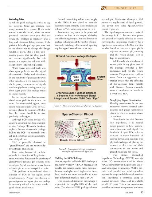
SparseChevron Pinout<br />
Grounds Powers Signals<br />
Figure 2 – <strong>Xilinx</strong> SparseChevron pinout places<br />
return pins adjacent to each signal pin.<br />
Tackling <strong>the</strong> SSN Challenge<br />
One package that tackles <strong>the</strong> SSN challenge is<br />
<strong>the</strong> <strong>Xilinx</strong> ® Virtex-4 FPGA package. Most<br />
notably, <strong>the</strong> package enables better noise performance<br />
on higher speed single-ended interfaces,<br />
which are more susceptible to noise<br />
than differential interfaces such as LVDS.<br />
The pinout architecture of <strong>the</strong> package is<br />
responsible for roughly 80% of <strong>the</strong> total<br />
noise. The Virtex-4 FPGA package achieves<br />
CONNECTIVITY<br />
optimal pin distribution through a tiled<br />
pattern – a regular array of signal, ground,<br />
and power pins called SparseChevron<br />
pinout (Figure 2).<br />
The signal-to-ground-to-power ratio of<br />
<strong>the</strong> package is 8:1:1. Because both power<br />
and ground are equally effective as return<br />
current paths, <strong>the</strong> package effectively has a<br />
signal-to-return ratio of 4:1. Also, <strong>the</strong> pins<br />
are distributed so that every signal pin is<br />
adjacent to a return pin, ensuring<br />
that <strong>the</strong> return current loop is<br />
kept to a minimum.<br />
Additionally, <strong>the</strong> abundance of<br />
return paths in any given area of<br />
<strong>the</strong> package provides a low<br />
impedance path for <strong>the</strong> return<br />
currents. The pinout also confines<br />
noise from an aggressor to a<br />
smaller area so that <strong>the</strong> influence<br />
of <strong>the</strong> aggressor drops rapidly<br />
with distance. Because crosstalk<br />
noise is cumulative, this results in<br />
a lower total SSN.<br />
Simplifying Signal Termination<br />
On-chip termination (active termination)<br />
removes external components<br />
and places termination<br />
closest to where it matters (driver<br />
or receiver).<br />
To maintain <strong>the</strong> ideal 50 ohm<br />
line impedance, it is normal<br />
design practice to have termination<br />
resistors on each signal. For<br />
hundreds of signal I/Os, this can<br />
translate to many hundreds of<br />
external termination resistors. The<br />
physical challenges of placing <strong>the</strong><br />
resistors on <strong>the</strong> board and <strong>the</strong>ir<br />
connections to <strong>the</strong> power and<br />
ground planes are not trivial.<br />
The <strong>Xilinx</strong> Controlled<br />
Impedance Technology (XCITE) on-chip<br />
active I/O termination used in Virtex<br />
FPGAs solves many of <strong>the</strong> problems associated<br />
with signal termination. XCITE provides<br />
both parallel and serial equivalent<br />
options for single and differential termination.<br />
Impedance is controlled using an<br />
internal reference voltage and is available<br />
on all I/O pins. This active termination<br />
provides automatic temperature and volt-<br />
Third Quarter 2005 Xcell Journal 83


