

Design Challenges: Avoiding the Pitfalls, winning the game - Xilinx
Design Challenges: Avoiding the Pitfalls, winning the game - Xilinx
Design Challenges: Avoiding the Pitfalls, winning the game - Xilinx

You also want an ePaper? Increase the reach of your titles
YUMPU automatically turns print PDFs into web optimized ePapers that Google loves.
Using Precision Sy<strong>the</strong>sis,<br />
Block Mult Post PnR<br />
Target Device LUTs Reg<br />
ISE 7.1_sp1 & DSP Timing<br />
Virtex-4 (1.5v, 90-nm<br />
copper process) 4VSX35ff668: 12 0 0 16 2.151ns<br />
Virtex-II Pro (1.5v, 0.13 µm,<br />
9-layer copper process) 2VP30ff1152: 7 720 1332 16 4.998ns<br />
Virtex-II (1.5v, 0.15/0.12 µm,<br />
8-layer metal process) 2V4000ff1152: 6 720 1332 16 6.905ns<br />
Virtex-E (1.8v, 0.18 µm metal,<br />
6-layer process) v3200efg1156: 8 8722 2165 0 16.005ns<br />
Virtex (2.5v, 0.22 µm,<br />
5-layer metal process) v800fg680: 6 8722 2165 0 20.704ns<br />
B<br />
A<br />
PCIN<br />
Table 1 – Precision Syn<strong>the</strong>sis post-place and route area and timing results<br />
X<br />
+<br />
0<br />
DSP48 SLICE<br />
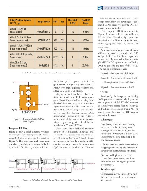
Figure 4 – A transposed MULT-ADD<br />
block diagram<br />
PCOUT<br />
Transposed FIR Filter<br />
Figure 2 shows a block diagram, whereas<br />
an example of <strong>the</strong> coding style of a transposed<br />
FIR filter structure is illustrated in<br />
Figure 3. The post-place and route area<br />
and timing results are in shown in Table<br />
1, in which Precision Syn<strong>the</strong>sis will infer<br />
<strong>the</strong> MULT_ADD operator (block diagram<br />
shown in Figure 4); map MULTI-<br />
PLIER with input-pipeline registers; and<br />
adder logic using DSP blocks.<br />
As you can see from Table 1, Precision<br />
Syn<strong>the</strong>sis uses <strong>the</strong> same RTL design to target<br />
different Virtex families, starting from<br />
<strong>the</strong> first Virtex device (2.5v, 0.22 µm, five<br />
layers metal process) to <strong>the</strong> latest Virtex-4<br />
device (1.5v, 90 nm copper process). You<br />
may notice that <strong>the</strong> exponential QoR<br />
improvement begins with <strong>the</strong> Virtex-II<br />
family; most of <strong>the</strong> improvement was contributed<br />
by <strong>the</strong> integration of a dedicated<br />
multiplier in Virtex-II FPGAs.<br />
Since <strong>the</strong>n, <strong>the</strong>se dedicated resources<br />
have been continuously enhanced and<br />
eventually transformed into <strong>the</strong> advanced<br />
DSP48 slice in <strong>the</strong> Virtex-4 family. Based<br />
on <strong>the</strong> results in Table 1, it would be difficult<br />
for anyone to doubt <strong>the</strong> tremendous<br />
QoR improvements that <strong>the</strong> Virtex-4<br />
Figure 5 – Technology schematic for <strong>the</strong> 16-tap transposed FIR filter design<br />
device has brought to today’s FPGA DSP<br />
design community. The advantages of dedicated<br />
DSP48 slices over discrete DSP elements<br />
are also quite clear.<br />
The transposed FIR filter structure in<br />
Figure 2 is optimal for use with <strong>the</strong><br />
DSP48 slice. Precision Syn<strong>the</strong>sis can<br />
absorb all FPGA fabric into DSP48 slices,<br />
including pipeline registers, adders, and<br />
multipliers.<br />
You may choose to use one of many<br />
different approaches to code this DSP<br />
design block. Let’s describe one approach<br />
where you only have to implement a simple<br />
MULT-ADD operator and use Verilog<br />
2001 to generate <strong>the</strong> rest of <strong>the</strong> blocks.<br />
The design specifications are:<br />
• Signed 18-bit input sampled (B(n))<br />
• Signed 18-bit input coefficients (h(n))<br />
– Use registers to store coefficients<br />
• Signed 48-bit output stream (P(n))<br />
• 16 taps<br />
SYSTEM PERFORMANCE<br />
Precision Syn<strong>the</strong>sis supports <strong>the</strong> Verilog<br />
2001 generate statement, which you can<br />
use to generate this MULT-ADD operator<br />
as shown by <strong>the</strong> coding example (Figure 3)<br />
and technology schematic (Figure 5). The<br />
pros to using <strong>the</strong> transposed FIR filter far<br />
outweigh <strong>the</strong> cons.<br />
Advantages:<br />
• Low latency – <strong>the</strong> maximum latency<br />
never exceeds <strong>the</strong> pipelining time<br />
through <strong>the</strong> slice containing <strong>the</strong> first<br />
coefficient. Typically, this is three clock<br />
cycles from <strong>the</strong> time data is input to<br />
<strong>the</strong> displayed result.<br />
• Efficient mapping to <strong>the</strong> DSP48 slice –<br />
mapping is enabled by <strong>the</strong> adder chain<br />
structure of <strong>the</strong> transposed FIR filter.<br />
• No external logic – no external<br />
FPGA fabric is required, enabling<br />
you to achieve <strong>the</strong> highest possible<br />
performance.<br />
Disadvantages:<br />
• Performance may be limited by a high<br />
fan-out input signal if a large number<br />
of taps exist.<br />
Third Quarter 2005 Xcell Journal 27


