TELE-TECH & - AmericanRadioHistory.Com
TELE-TECH & - AmericanRadioHistory.Com
TELE-TECH & - AmericanRadioHistory.Com

You also want an ePaper? Increase the reach of your titles
YUMPU automatically turns print PDFs into web optimized ePapers that Google loves.
By W. F. CHOW<br />
Meter<br />
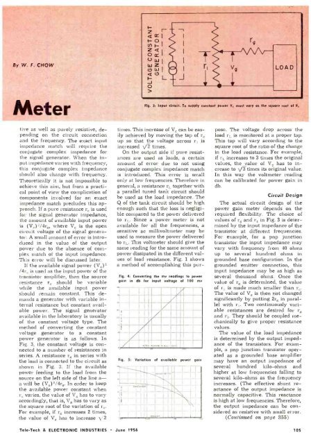
Fig.<br />
3: Input circuit. To supply constant power V, must vary as the square root of R,<br />
tive as well as purely resistive, depending<br />
on the circuit connection<br />
and the frequency. The exact input<br />
impedance match will require the<br />
conjugate complex impedance for<br />
the signal generator. When the input<br />
impedance varies with frequency,<br />
this conjugate complex impedance<br />
should also change with frequency.<br />
Theoretically it is not impossible to<br />
achieve this aim, but from a practical<br />
point of view the complication of<br />
components involved for an exact<br />
impedance match precludes this approach.<br />
If a pure resistance r,, is used<br />
for the signal generator impedance,<br />
the amount of available input power<br />
is (VF)2 /4rF, where V is the open<br />
circuit voltage of the signal generator.<br />
A small amount of error is introduced<br />
in the value of the output<br />
power due to the absence of complex<br />
match of the input impedance.<br />
This error will be discussed later.<br />
If the available signal power (VF)2<br />
/4r is used as the input power of the<br />
transistor amplifier, then the source<br />
resistance rF should be variable<br />
while the available input power<br />
should remain constant. This demands<br />
a generator with variable internal<br />
resistance but constant available<br />
power. The signal generator<br />
available in the laboratory is usually<br />
of the constant voltage type. The<br />
method of converting the constant<br />
voltage generator to a constant<br />
power generator is as follows. In<br />
Fig. 3. the constant voltage is connected<br />
to a number of resistances in<br />
series. A resistance rF in series with<br />
the load is connected to the circuit as<br />
shown in Fig. 3. If the available<br />
power feeding to the load from the<br />
source on the left side of the line a-<br />
a will be (VF)2 /4rF. In order to keep<br />
the available power constant when<br />
r,, varies, the value of VF has to vary<br />
accordingly, that is, VF has to vary as<br />
the square root of the variation of rF.<br />
For example, if rF increases 2 times,<br />
the value of V_, has to increase \'2<br />
times. This increase of VF can be easily<br />
achieved by moving the tap of rg<br />
up so that the voltage across r, is<br />
increased V/2 times.<br />
On the output side if pure resistances<br />
are used as loads, a certain<br />
amount of error due to not using<br />
conjugate complex impedance match<br />
is introduced. This error is small<br />
only at low frequencies. Therefore in<br />
general, a resistance r,, together with<br />
a parallel tuned tank circuit should<br />
be used as the load impedance. The<br />
Q of the tank circuit should be high<br />
enough such that the loss is negligible<br />
compared to the power delivered<br />
to r1,. Since a power meter is not<br />
available for all the frequencies, a<br />
sensitive ac millivoltmeter may be<br />
used to measure the power delivered<br />
to r,,. This voltmeter should give the<br />
same reading for the same amount of<br />
power dissipated in the different values<br />
of load resistance. Fig. 1 shows<br />
a method of accomplishing this pur-<br />
ZS<br />
Fig. 4: Converting the my readings to power<br />
gain in db for input voltage of 100 my<br />
ZO<br />
n1NNIIIMI<br />
111111/1111N<br />
11121111111<br />
AMIN n<br />
Fig. 5: Variation of available power gain<br />
pose. The voltage drop across the<br />
load r,, is monitored at a proper tap.<br />
This tap will vary according to the<br />
square root of the ratio of the change<br />
in the load resistance. For example,<br />
if r,, increases to 3 times the original<br />
values, the value of V. has to increase<br />
to \/3 times its original value.<br />
In this way the voltmeter reading<br />
can be calibrated for power gain in<br />
db.<br />
Circuit Design<br />
The actual circuit design of the<br />
power gain meter depends on the<br />
required flexibility. The choice of<br />
values of r, and r, in Fig. 3 is determined<br />
by the input impedance of the<br />
transistor at different frequencies.<br />
For example, for a pnp junction<br />
transistor the input impedance may<br />
vary with frequency from 40 ohms<br />
up to several hundred ohms in<br />
grounded base configuration. In the<br />
grounded emitter connection, this<br />
input impedance may be as high as<br />
several thousand ohms. Once the<br />
value of rF is determined, the value<br />
of r, is made much smaller than r,;.<br />
The value of VF is then riot changed<br />
significantly by putting 2r, in parallel<br />
with r,. Two continuously variable<br />
resistances are desired for rF<br />
and r1. They should be coupled mechanically<br />
to give proper resistance<br />
values.<br />
The value of the load impedance<br />
is determined by the output impedance<br />
of the transistors. For example,<br />
a pnp junction transistor operated<br />
as a grounded base amplifier<br />
may have an output impedance of<br />
several hundred kilo -ohms and<br />
higher at low frequencies falling to<br />
several kilo -ohms as the frequency<br />
increases. (The effective shunt reactance<br />
of the output impedance is<br />
normally capacitive. This reactance<br />
is high at low frequencies. Therefore,<br />
the output impedance can be considered<br />
as resistive with small error.<br />
(Continued on page 355)<br />
Tele -Tech & ELECTRONIC INDUSTRIES June 1956<br />
105