3.22EjemploDRM007 Co..
3.22EjemploDRM007 Co..
3.22EjemploDRM007 Co..

You also want an ePaper? Increase the reach of your titles
YUMPU automatically turns print PDFs into web optimized ePapers that Google loves.
Software Design <strong>Co</strong>nsiderations<br />
Data Flow<br />
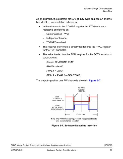
As an example, the algorithm for 50% of duty cycle on phase A and the<br />
two MOSFET commutation scheme is:<br />
• In the microcontroller CONFIG register the PWM write once<br />
register is configured as:<br />
– Center aligned PWM<br />
– Independent mode<br />
– TOPNEG enabled<br />
• The required duty cycle is directly loaded into the PVAL register<br />
for the TOP transistor.<br />
• The value loaded into the PVAL register for the BOT transistor is<br />
calculated as:<br />
#define DEADTIME 0x10<br />
PMOD = 0x100;<br />
PVAL1 = 0x80;<br />
PVAL2 = PVAL1 – DEADTIME;<br />
The output signal for one PWM cycle is shown in Figure 5-7.<br />
SOFTWARE<br />
DEADTIME<br />
INSERTION<br />
PWM1<br />
TOP MOSFET<br />
TOPNEG ENABLED<br />
PWM2<br />
BOTTOM MOSFET<br />
BOTNEG DISABLED<br />
1 CYCLE PWM<br />
Note: The PWMMC is configured with independent mode<br />
and center aligned operation<br />
Figure 5-7. Software Deadtime Insertion<br />
BLDC Motor <strong>Co</strong>ntrol Board for Industrial and Appliance Applications<br />
DRM007<br />
MOTOROLA Software Design <strong>Co</strong>nsiderations 85